

Encyclopedia Entry: 74ALVCH32374BFG
Product Overview
Category
The 74ALVCH32374BFG belongs to the category of integrated circuits (ICs) and specifically falls under the family of flip-flops.
Use
This product is primarily used for storing digital information in electronic systems. It serves as a latch or register, allowing data to be stored and retrieved as needed.
Characteristics
- The 74ALVCH32374BFG is a high-performance, low-power, 32-bit D-type flip-flop.
- It operates at a voltage range of 1.65V to 3.6V, making it suitable for various applications.
- This IC offers high-speed operation with a maximum propagation delay of 2.5 ns.
- It features a wide operating temperature range, typically from -40°C to +85°C.
- The 74ALVCH32374BFG is designed to have low power consumption, making it energy-efficient.
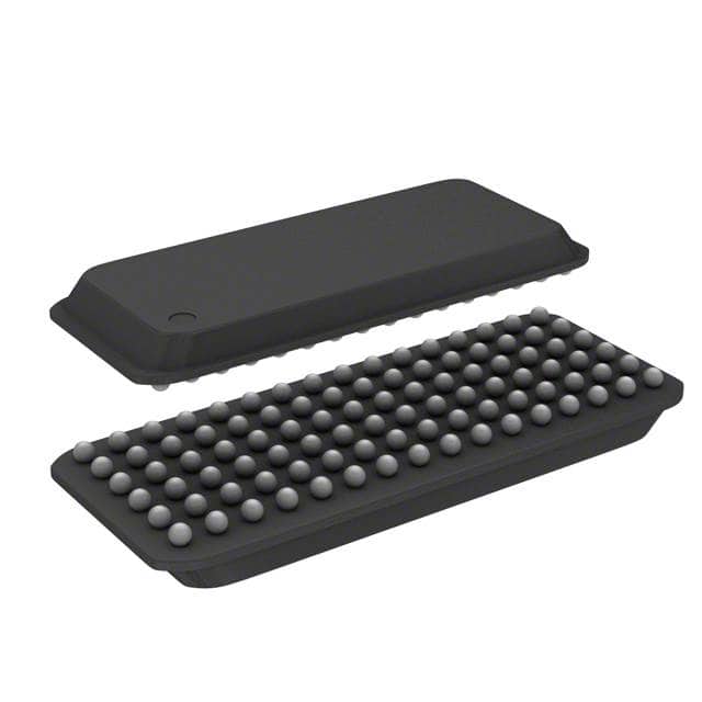
Package and Quantity
This product is available in a small-outline integrated circuit (SOIC) package. Each package contains one 74ALVCH32374BFG IC.
Essence
The essence of the 74ALVCH32374BFG lies in its ability to store and retain digital data reliably, providing a crucial component for sequential logic operations in electronic systems.
Specifications
- Number of Flip-Flops: 32
- Input Voltage Range: 0V to VCC
- Output Voltage Range: 0V to VCC
- Maximum Clock Frequency: 200 MHz
- Input Capacitance: 4 pF
- Output Capacitance: 8 pF
- Supply Voltage Range: 1.65V to 3.6V
- Operating Temperature Range: -40°C to +85°C
Detailed Pin Configuration
The 74ALVCH32374BFG has a total of 48 pins, which are assigned specific functions. Here is the detailed pin configuration:
- Pin 1: Output Q0
- Pin 2: Output Q0 (bar)
- Pin 3: Clock Input (CLK)
- Pin 4: Data Input D0
- Pin 5: Data Input D0 (bar)
- Pin 6: Data Input D1
- Pin 7: Data Input D1 (bar)
- Pin 8: GND (Ground)
- Pin 9: Data Input D2
- Pin 10: Data Input D2 (bar)
- Pin 11: Data Input D3
- Pin 12: Data Input D3 (bar)
- Pin 13: Data Input D4
- Pin 14: Data Input D4 (bar)
- Pin 15: Data Input D5
- Pin 16: Data Input D5 (bar)
- Pin 17: Data Input D6
- Pin 18: Data Input D6 (bar)
- Pin 19: Data Input D7
- Pin 20: Data Input D7 (bar)
- Pin 21: VCC (Supply Voltage)
- Pin 22: Output Q1
- Pin 23: Output Q1 (bar)
- Pin 24: Output Enable (OE)
- Pin 25: Output Q2
- Pin 26: Output Q2 (bar)
- Pin 27: Output Q3
- Pin 28: Output Q3 (bar)
- Pin 29: Output Q4
- Pin 30: Output Q4 (bar)
- Pin 31: Output Q5
- Pin 32: Output Q5 (bar)
- Pin 33: Output Q6
- Pin 34: Output Q6 (bar)
- Pin 35: Output Q7
- Pin 36: Output Q7 (bar)
- Pin 37: Output Q8
- Pin 38: Output Q8 (bar)
- Pin 39: Output Q9
- Pin 40: Output Q9 (bar)
- Pin 41: Output Q10
- Pin 42: Output Q10 (bar)
- Pin 43: Output Q11
- Pin 44: Output Q11 (bar)
- Pin 45: Output Q12
- Pin 46: Output Q12 (bar)
- Pin 47: Output Q13
- Pin 48: Output Q13 (bar)
Functional Features
- The 74ALVCH32374BFG operates as a positive-edge-triggered flip-flop.
- It has an output enable pin (OE) that allows
技術ソリューションにおける 74ALVCH32374BFG の適用に関連する 10 件の一般的な質問と回答をリストします。
Sure! Here are 10 common questions and answers related to the application of 74ALVCH32374BFG in technical solutions:
Q: What is the function of the 74ALVCH32374BFG?
- A: The 74ALVCH32374BFG is an octal D-type flip-flop with 3-state outputs. It can store and transfer data in digital systems.
Q: What is the operating voltage range for this IC?
- A: The 74ALVCH32374BFG operates within a voltage range of 1.65V to 3.6V.
Q: How many flip-flops are there in the 74ALVCH32374BFG?
- A: This IC contains 8 flip-flops, making it an octal flip-flop.
Q: What is the maximum clock frequency supported by this IC?
- A: The 74ALVCH32374BFG can operate at a maximum clock frequency of 200 MHz.
Q: Can I use this IC in both synchronous and asynchronous applications?
- A: Yes, the 74ALVCH32374BFG can be used in both synchronous and asynchronous applications.
Q: What is the output drive strength of this IC?
- A: The 74ALVCH32374BFG has a typical output drive strength of ±24 mA.
Q: Does this IC have any power-saving features?
- A: Yes, the 74ALVCH32374BFG has a power-down mode that reduces power consumption when not in use.
Q: Can I cascade multiple 74ALVCH32374BFG ICs together?
- A: Yes, you can cascade multiple ICs to increase the number of flip-flops in your system.
Q: What is the propagation delay of this IC?
- A: The propagation delay of the 74ALVCH32374BFG is typically around 2.5 ns.
Q: Are there any specific precautions I need to take while using this IC?
- A: It is recommended to follow the manufacturer's datasheet for proper handling, power supply decoupling, and signal integrity considerations.
Please note that these answers are general and may vary depending on the specific datasheet and application requirements.