

PI6CFGL402BLIE
Overview
- Category: Integrated Circuit
- Use: Signal Conditioning and Clock Generation
- Characteristics: Low Jitter, High-Speed, Low Power Consumption
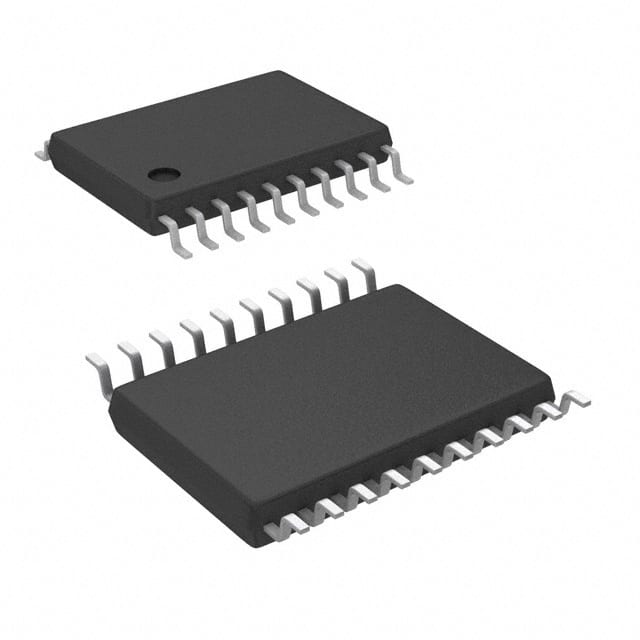
- Package: QFN (Quad Flat No-Lead)
- Essence: Clock Buffer and Fanout Driver
- Packaging/Quantity: Tape and Reel, 2500 units per reel
Specifications and Parameters
- Supply Voltage: 3.3V
- Input Frequency Range: 1MHz - 400MHz
- Output Frequency Range: 1MHz - 400MHz
- Number of Outputs: 4
- Output Type: LVCMOS
- Operating Temperature Range: -40°C to +85°C
Pin Configuration
The PI6CFGL402BLIE has the following pin configuration:
- VDD
- GND
- CLKIN
- CLKOUT0
- CLKOUT1
- CLKOUT2
- CLKOUT3
- OE#
Functional Characteristics
- Provides low jitter clock distribution for high-speed systems.
- Acts as a fanout driver, enabling multiple outputs from a single input clock signal.
- Supports LVCMOS output signaling.
- Offers excellent signal integrity and minimal skew.
Advantages and Disadvantages
Advantages: - Low power consumption. - Wide operating temperature range. - Small package size. - High-speed performance.
Disadvantages: - Limited number of outputs. - Restricted frequency range.
Applicable Range of Products
The PI6CFGL402BLIE is suitable for various applications, including: - Networking equipment - Data storage devices - Communication systems - Industrial automation
Working Principles
The PI6CFGL402BLIE receives an input clock signal (CLKIN) and generates four synchronized output clock signals (CLKOUT0, CLKOUT1, CLKOUT2, CLKOUT3). It conditions and buffers the input signal to minimize jitter and distortion, ensuring reliable clock distribution throughout the system.
Detailed Application Field Plans
The PI6CFGL402BLIE can be used in the following application fields:
Networking Equipment:
- Ethernet switches
- Routers
- Network interface cards
Data Storage Devices:
- Solid-state drives (SSDs)
- Hard disk drives (HDDs)
- RAID controllers
Communication Systems:
- Wireless base stations
- Satellite communication systems
- Cellular network infrastructure
Industrial Automation:
- Programmable logic controllers (PLCs)
- Motor control systems
- Robotics
Detailed Alternative Models
Some alternative models to the PI6CFGL402BLIE are:
- PI6CFGL403BLIE
- PI6CFGL404BLIE
- PI6CFGL405BLIE
5 Common Technical Questions and Answers
Q: What is the maximum operating frequency of the PI6CFGL402BLIE? A: The maximum operating frequency is 400MHz.
Q: Can I use this IC with a 5V power supply? A: No, the PI6CFGL402BLIE requires a 3.3V power supply.
Q: How many outputs does this IC have? A: The PI6CFGL402BLIE has four outputs.
Q: What is the package type of this IC? A: It comes in a QFN (Quad Flat No-Lead) package.
Q: What is the typical power consumption of this IC? A: The typical power consumption is low, thanks to its efficient design.
This encyclopedia entry provides an overview of the PI6CFGL402BLIE integrated circuit, including its category, use, characteristics, package, specifications, pin configuration, functional characteristics, advantages and disadvantages, applicable range of products, working principles, detailed application field plans, alternative models, and common technical questions and answers.