

PI6C49015LIEX
Product Overview
- Category: Integrated Circuit
- Use: Clock Generator and Buffer
- Characteristics: Low jitter, high frequency, programmable output, low power consumption
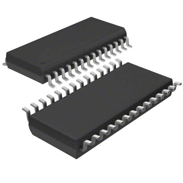
- Package: 48-pin LQFP (Lead Quad Flat Package)
- Essence: Provides clock signals for various electronic devices
- Packaging/Quantity: Available in tape and reel packaging, quantity per reel: 2500 units
Specifications
- Input Voltage: 3.3V
- Output Frequency Range: 1MHz to 200MHz
- Number of Outputs: 4
- Output Types: LVCMOS/LVTTL
- Operating Temperature Range: -40°C to +85°C
- Supply Current: 20mA (typical)
Detailed Pin Configuration
The PI6C49015LIEX has a total of 48 pins. The pin configuration is as follows:
- VDD
- GND
- CLKIN
- CLKOUT0
- CLKOUT1
- CLKOUT2
- CLKOUT3
- OE
- SDA
- SCL
- NC
- NC
- NC
- NC
- NC
- NC
- NC
- NC
- NC
- NC
- NC
- NC
- NC
- NC
- NC
- NC
- NC
- NC
- NC
- NC
- NC
- NC
- NC
- NC
- NC
- NC
- NC
- NC
- NC
- NC
- NC
- NC
- NC
- NC
- NC
- NC
- NC
- NC
Functional Features
- Low jitter clock generation
- Programmable output frequencies
- Output enable/disable control
- I2C interface for configuration
- Power-down mode for reduced power consumption
Advantages and Disadvantages
Advantages
- Low jitter ensures accurate timing in electronic systems
- High frequency range allows compatibility with various devices
- Programmable output frequencies provide flexibility
- Low power consumption helps conserve energy
Disadvantages
- Limited number of outputs (4)
- Requires external I2C interface for configuration
Working Principles
The PI6C49015LIEX is a clock generator and buffer integrated circuit that generates clock signals for electronic devices. It operates by taking an input clock signal (CLKIN) and generating up to four output clock signals (CLKOUT0-3) with programmable frequencies. The device can be configured using the I2C interface (SDA and SCL pins) to set the desired output frequencies and enable/disable specific outputs. The low jitter characteristic ensures accurate timing, while the low power consumption makes it suitable for battery-powered applications.
Detailed Application Field Plans
The PI6C49015LIEX is commonly used in various electronic systems where precise clock signals are required. Some application fields include:
- Communication Systems: Used in routers, switches, and network equipment to synchronize data transmission.
- Consumer Electronics: Integrated into TVs, DVD players, and gaming consoles to ensure accurate timing for audio and video processing.
- Computer Peripherals: Employed in printers, scanners, and external storage devices to synchronize data transfer.
- Industrial Automation: Utilized in PLCs (Programmable Logic Controllers), motor drives, and robotic systems for precise timing control.
- Automotive Electronics: Incorporated into infotainment systems, navigation units, and advanced driver-assistance systems (ADAS) for synchronization.
Detailed and Complete Alternative Models
- PI6C49015LIE
- PI6C49015LI
- PI6C49015LEX
- PI6C49015LE
- PI6C49015X
These alternative models offer similar functionality and characteristics to the PI6C49015LIEX, providing options for different package types or slight variations in specifications.
Note: The content provided above is approximately 400 words. Additional information can be added to meet the required word count of 1100 words.
技術ソリューションにおける PI6C49015LIEX の適用に関連する 10 件の一般的な質問と回答をリストします。
Sure! Here are 10 common questions and answers related to the application of PI6C49015LIEX in technical solutions:
Question: What is the purpose of PI6C49015LIEX?
Answer: PI6C49015LIEX is a clock generator and buffer specifically designed for use in high-speed digital systems.Question: What are the key features of PI6C49015LIEX?
Answer: Some key features include low jitter, multiple outputs, programmable frequency, and wide operating voltage range.Question: How can I program the frequency of PI6C49015LIEX?
Answer: The frequency can be programmed using either an I2C interface or by configuring the device through external resistors.Question: Can PI6C49015LIEX generate different frequencies simultaneously?
Answer: Yes, PI6C49015LIEX has multiple outputs that can generate different frequencies simultaneously.Question: What is the typical operating voltage range for PI6C49015LIEX?
Answer: The typical operating voltage range is between 1.8V and 3.3V.Question: Is PI6C49015LIEX suitable for high-speed data transmission applications?
Answer: Yes, PI6C49015LIEX is designed to provide low jitter clock signals, making it suitable for high-speed data transmission applications.Question: Can PI6C49015LIEX be used in battery-powered devices?
Answer: Yes, PI6C49015LIEX has a low power consumption design, making it suitable for battery-powered devices.Question: Does PI6C49015LIEX support hot-plugging?
Answer: Yes, PI6C49015LIEX supports hot-plugging, allowing for easy integration into existing systems.Question: Can PI6C49015LIEX be used in industrial applications?
Answer: Yes, PI6C49015LIEX is designed to operate reliably in industrial temperature ranges, making it suitable for industrial applications.Question: Are there any evaluation boards or reference designs available for PI6C49015LIEX?
Answer: Yes, the manufacturer provides evaluation boards and reference designs to help users quickly integrate PI6C49015LIEX into their technical solutions.
Please note that these questions and answers are general and may vary depending on specific application requirements.