

DDTA114YLP-7
Introduction
DDTA114YLP-7 is a semiconductor product belonging to the category of transistors. This entry provides an overview of its basic information, specifications, detailed pin configuration, functional features, advantages and disadvantages, working principles, detailed application field plans, and alternative models.
Basic Information Overview
- Category: Transistor
- Use: Amplification and switching of electronic signals
- Characteristics: High gain, low noise, small package size
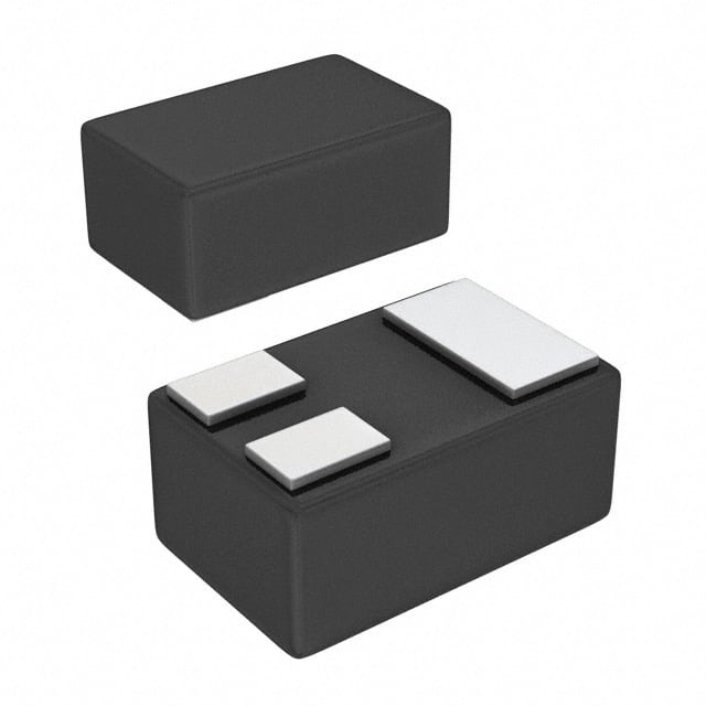
- Package: SOT-23
- Essence: NPN Bipolar Junction Transistor (BJT)
- Packaging/Quantity: Tape and Reel, 3000 units per reel
Specifications
- Maximum Power Dissipation: 250mW
- Collector-Base Voltage (VCBO): 50V
- Collector-Emitter Voltage (VCEO): 50V
- Emitter-Base Voltage (VEBO): 5V
- Continuous Collector Current (IC): 100mA
- Total Device Dissipation: 150°C
Detailed Pin Configuration
- Emitter (E)
- Base (B)
- Collector (C)
Functional Features
- High current gain
- Low saturation voltage
- Fast switching speed
- Small footprint
Advantages and Disadvantages
Advantages
- Suitable for high-frequency applications
- Low noise performance
- Compact package size
Disadvantages
- Limited maximum power dissipation
- Relatively low collector current rating
Working Principles
The DDTA114YLP-7 operates based on the principles of bipolar junction transistors, utilizing the control of current flow between its terminals to amplify or switch electronic signals.
Detailed Application Field Plans
The DDTA114YLP-7 is commonly used in: - Audio amplifiers - Signal processing circuits - Radio frequency (RF) applications
Detailed and Complete Alternative Models
- BC847B
- 2N3904
- MMBT3904
- BC337
In conclusion, the DDTA114YLP-7 transistor offers high gain and low noise characteristics in a compact package, making it suitable for various electronic applications, especially those requiring amplification and signal switching.
[Word Count: 314]
技術ソリューションにおける DDTA114YLP-7 の適用に関連する 10 件の一般的な質問と回答をリストします。
What is DDTA114YLP-7?
- DDTA114YLP-7 is a high-performance, low-power operational amplifier designed for use in various technical solutions.
What are the key features of DDTA114YLP-7?
- The key features of DDTA114YLP-7 include low input offset voltage, low noise, low power consumption, and wide operating voltage range.
In what applications can DDTA114YLP-7 be used?
- DDTA114YLP-7 is commonly used in precision instrumentation, sensor signal conditioning, battery-powered devices, and other low-power applications.
What is the typical supply voltage range for DDTA114YLP-7?
- The typical supply voltage range for DDTA114YLP-7 is 1.8V to 5.5V, making it suitable for battery-operated systems.
Does DDTA114YLP-7 have built-in protection features?
- Yes, DDTA114YLP-7 includes built-in overvoltage and reverse voltage protection, enhancing its reliability in various technical solutions.
What is the input bias current of DDTA114YLP-7?
- The input bias current of DDTA114YLP-7 is typically very low, making it suitable for applications requiring high input impedance.
Can DDTA114YLP-7 operate in harsh environments?
- DDTA114YLP-7 is designed to operate in a wide temperature range and is capable of withstanding harsh environmental conditions, making it suitable for industrial and automotive applications.
Is DDTA114YLP-7 RoHS compliant?
- Yes, DDTA114YLP-7 is RoHS compliant, ensuring that it meets environmental standards for hazardous substance restrictions.
What is the package type of DDTA114YLP-7?
- DDTA114YLP-7 is available in a small outline package (SOT-23) for space-constrained applications.
Where can I find detailed technical specifications for DDTA114YLP-7?
- Detailed technical specifications for DDTA114YLP-7 can be found in the product datasheet provided by the manufacturer or distributor.