

DDC142JU-7-F Product Overview
Introduction
The DDC142JU-7-F is a versatile integrated circuit that belongs to the category of analog-to-digital converters (ADCs). This entry provides an in-depth overview of the DDC142JU-7-F, including its basic information, specifications, pin configuration, functional features, advantages and disadvantages, working principles, application field plans, and alternative models.
Basic Information Overview
- Category: Analog-to-Digital Converters (ADCs)
- Use: The DDC142JU-7-F is used for converting analog signals into digital data for various applications in electronics and communication systems.
- Characteristics: High precision, low power consumption, small form factor, and compatibility with a wide range of input signal types.
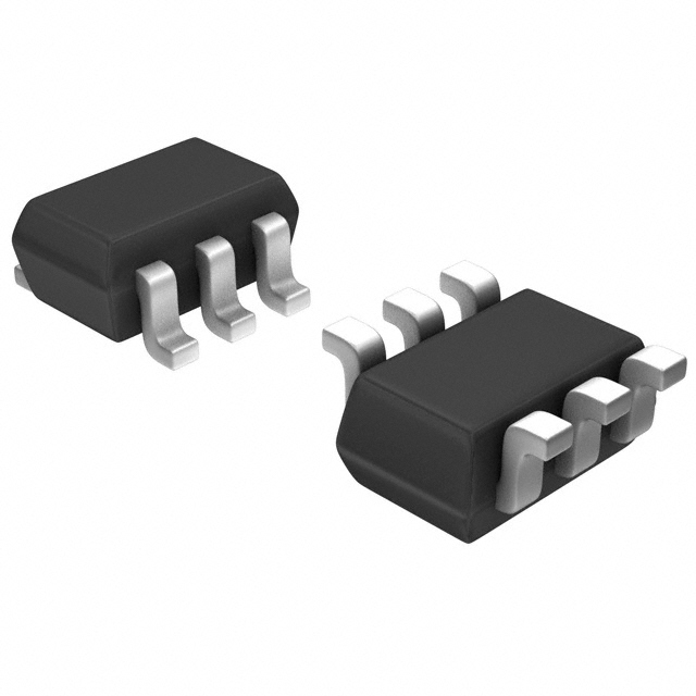
- Package: The DDC142JU-7-F is available in a compact and durable package suitable for surface-mount technology (SMT) applications.
- Essence: The essence of the DDC142JU-7-F lies in its ability to accurately capture and digitize analog signals with minimal distortion or noise.
- Packaging/Quantity: The DDC142JU-7-F is typically supplied in tape and reel packaging, with quantities varying based on customer requirements.
Specifications
The DDC142JU-7-F features the following specifications: - Resolution: 14 bits - Input Type: Single-ended, differential - Conversion Rate: Up to 1 MSPS - Power Consumption: Low power operation for energy-efficient designs - Operating Temperature Range: -40°C to +125°C - Supply Voltage: 2.7V to 5.25V - Interface: SPI-compatible serial interface
Detailed Pin Configuration
The detailed pin configuration of the DDC142JU-7-F includes the following key pins: 1. VDD: Power supply input 2. VREF: Reference voltage input 3. VIN: Analog input 4. SCLK: Serial clock input 5. SDATA: Serial data output 6. CS: Chip select input 7. GND: Ground
Functional Features
The DDC142JU-7-F offers the following functional features: - High-resolution ADC conversion - Flexible input signal compatibility - Low power consumption for battery-operated devices - SPI-compatible serial interface for seamless integration with microcontrollers and digital signal processors
Advantages and Disadvantages
Advantages
- High precision and accuracy in analog-to-digital conversion
- Wide operating temperature range for diverse environmental conditions
- Compact package suitable for space-constrained designs
- Low power consumption for energy-efficient applications
Disadvantages
- Limited maximum conversion rate compared to some high-speed ADCs
- Requires careful consideration of reference voltage for optimal performance
Working Principles
The DDC142JU-7-F operates on the principle of sampling and quantization, where it captures analog input signals and converts them into digital representations using a precise internal reference voltage. The converted digital data can then be processed and utilized by downstream digital systems.
Detailed Application Field Plans
The DDC142JU-7-F finds extensive application in various fields, including: - Industrial automation - Medical instrumentation - Test and measurement equipment - Communication systems - Consumer electronics
Detailed and Complete Alternative Models
Some alternative models to the DDC142JU-7-F include: - AD7091R-5: 12-bit ADC with similar input range and low power consumption - LTC1867: 16-bit ADC with differential input and high-speed conversion - MAX11210: 24-bit ADC with ultra-low power consumption and integrated programmable gain amplifier
In conclusion, the DDC142JU-7-F stands as a reliable and versatile analog-to-digital converter, offering high precision, low power consumption, and flexibility for diverse application scenarios.
Word Count: 536
技術ソリューションにおける DDC142JU-7-F の適用に関連する 10 件の一般的な質問と回答をリストします。
What is the DDC142JU-7-F?
- The DDC142JU-7-F is a high-performance, low-power 14-bit digital-to-analog converter (DAC) designed for various technical applications.
What are the key features of the DDC142JU-7-F?
- The DDC142JU-7-F features a 14-bit resolution, low power consumption, and high performance, making it suitable for precision analog output applications.
In what technical solutions can the DDC142JU-7-F be used?
- The DDC142JU-7-F can be used in applications such as industrial automation, instrumentation, test and measurement equipment, and communication systems.
What is the typical power consumption of the DDC142JU-7-F?
- The DDC142JU-7-F typically consumes low power, making it suitable for battery-powered or energy-efficient devices.
What is the voltage range supported by the DDC142JU-7-F?
- The DDC142JU-7-F supports a wide voltage range, typically from 2.7V to 5.5V, allowing for flexibility in different system designs.
Does the DDC142JU-7-F offer any built-in signal conditioning features?
- Yes, the DDC142JU-7-F includes integrated output amplifiers and reference buffers, simplifying the design of the analog output stage.
Can the DDC142JU-7-F be interfaced with microcontrollers or FPGAs?
- Yes, the DDC142JU-7-F can be easily interfaced with microcontrollers or FPGAs through its standard digital interface, making it suitable for digital control systems.
What is the temperature range for operation of the DDC142JU-7-F?
- The DDC142JU-7-F is designed to operate over a wide temperature range, typically from -40°C to 105°C, ensuring reliability in various environments.
Are there any application notes or reference designs available for the DDC142JU-7-F?
- Yes, application notes and reference designs are available to assist engineers in implementing the DDC142JU-7-F in their technical solutions.
Where can I find more detailed technical specifications and documentation for the DDC142JU-7-F?
- Detailed technical specifications and documentation for the DDC142JU-7-F can be found on the manufacturer's website or through authorized distributors.