

Encyclopedia Entry: 74LVC2G34FZ4-7
Product Overview
Category
The 74LVC2G34FZ4-7 belongs to the category of integrated circuits (ICs).
Use
This IC is commonly used in electronic devices for signal amplification and buffering purposes.
Characteristics
- Low-voltage CMOS technology
- High-speed operation
- Wide operating voltage range
- Low power consumption
- Schmitt trigger inputs for noise immunity
Package
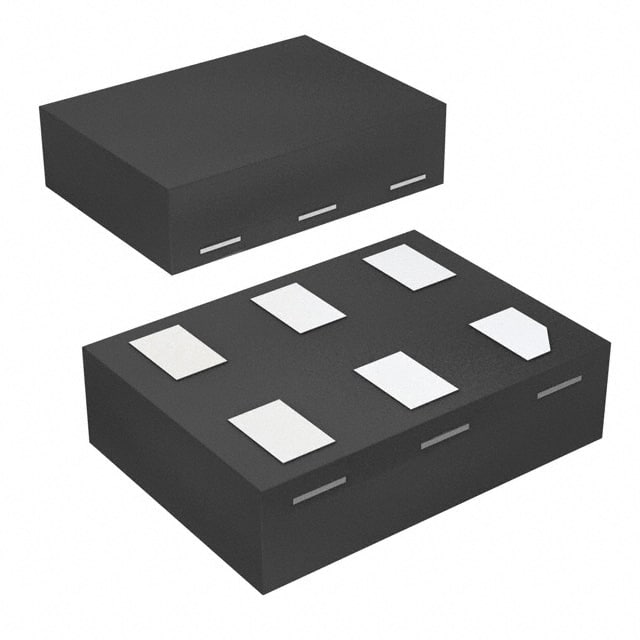
The 74LVC2G34FZ4-7 is available in a small form-factor package, such as SOT353 or DFN8.
Essence
The essence of this product lies in its ability to provide reliable signal amplification and buffering in various electronic applications.
Packaging/Quantity
The 74LVC2G34FZ4-7 is typically packaged in reels or tubes, with a quantity of 3000 units per reel/tube.
Specifications
- Supply Voltage Range: 1.65V to 5.5V
- Input Voltage Range: GND to VCC
- Output Voltage Range: GND to VCC
- Operating Temperature Range: -40°C to +85°C
- Maximum Propagation Delay: 3.5ns (typical)
- Maximum Quiescent Current: 10μA (typical)
Detailed Pin Configuration
The 74LVC2G34FZ4-7 has a total of 8 pins arranged as follows:
___________
   Y1 -|           |- VCC
   A1 -|           |- B1
   A2 -|           |- B2
   GND -|           |- Y2
        |___________|
Functional Features
- Dual buffer gates with Schmitt-trigger inputs
- Non-inverting logic function
- High-speed operation for signal amplification
- Wide operating voltage range allows compatibility with various systems
- Low power consumption for energy-efficient designs
- Schmitt trigger inputs provide noise immunity and hysteresis
Advantages and Disadvantages
Advantages
- Compact size enables integration into space-constrained designs
- Low-voltage operation reduces power requirements
- High-speed operation ensures efficient signal processing
- Noise immunity provided by Schmitt trigger inputs enhances reliability
Disadvantages
- Limited number of buffer gates in a single package
- May require additional external components for specific applications
Working Principles
The 74LVC2G34FZ4-7 operates based on CMOS technology, which allows for low-voltage operation. It consists of two buffer gates that amplify and buffer input signals. The Schmitt trigger inputs ensure noise immunity and hysteresis, making the IC suitable for applications where signal integrity is crucial.
Detailed Application Field Plans
The 74LVC2G34FZ4-7 finds application in various electronic devices and systems, including: 1. Communication equipment 2. Consumer electronics 3. Industrial automation 4. Automotive electronics 5. Medical devices
Detailed and Complete Alternative Models
- 74LVC2G04: Dual inverter gate IC
- 74LVC2G08: Dual AND gate IC
- 74LVC2G32: Dual OR gate IC
- 74LVC2G86: Dual XOR gate IC
These alternative models offer similar functionality and can be used as substitutes for the 74LVC2G34FZ4-7 depending on specific design requirements.
In conclusion, the 74LVC2G34FZ4-7 is a versatile integrated circuit that provides reliable signal amplification and buffering in various electronic applications. Its compact size, low-voltage operation, high-speed performance, and noise immunity make it a valuable component in modern electronic designs.
Word count: 420
技術ソリューションにおける 74LVC2G34FZ4-7 の適用に関連する 10 件の一般的な質問と回答をリストします。
Sure! Here are 10 common questions and answers related to the application of the 74LVC2G34FZ4-7 in technical solutions:
Q: What is the 74LVC2G34FZ4-7? A: The 74LVC2G34FZ4-7 is a dual buffer gate IC (Integrated Circuit) with Schmitt-trigger inputs.
Q: What is the purpose of the Schmitt-trigger inputs in this IC? A: The Schmitt-trigger inputs help provide hysteresis, making the IC less sensitive to noise and ensuring reliable switching.
Q: What voltage levels does the 74LVC2G34FZ4-7 support? A: The IC supports voltage levels from 1.65V to 5.5V, making it compatible with a wide range of systems.
Q: Can the 74LVC2G34FZ4-7 be used for level shifting applications? A: Yes, the IC can be used for level shifting between different voltage domains within a system.
Q: How many buffers are there in the 74LVC2G34FZ4-7? A: The IC has two independent buffer gates, allowing for separate signal buffering.
Q: What is the maximum output current of the 74LVC2G34FZ4-7? A: The IC can source or sink up to 32mA of current per output.
Q: Is the 74LVC2G34FZ4-7 suitable for high-speed applications? A: Yes, the IC has a propagation delay of only a few nanoseconds, making it suitable for high-speed digital circuits.
Q: Can the 74LVC2G34FZ4-7 be used in battery-powered devices? A: Yes, the IC has a low power consumption and can operate at lower supply voltages, making it suitable for battery-powered applications.
Q: Does the 74LVC2G34FZ4-7 have any built-in protection features? A: Yes, the IC has built-in ESD (Electrostatic Discharge) protection, providing robustness against electrostatic events.
Q: What package options are available for the 74LVC2G34FZ4-7? A: The IC is available in various package options, such as SOT353, XSON6, and DFN6, allowing for flexibility in board layout and design.
Please note that these answers are general and may vary depending on the specific application and requirements.