

74LVC2G125RA3-7
Basic Information Overview
- Category: Integrated Circuit (IC)
- Use: Buffer/Driver
- Characteristics: Dual Bus Buffer with 3-State Outputs
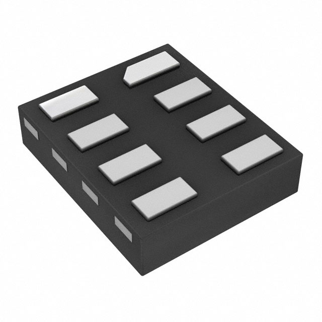
- Package: SOT753 (SC-70)
- Essence: Logic Level Shifter
- Packaging/Quantity: Tape and Reel, 3000 pieces per reel
Specifications
- Supply Voltage Range: 1.65V to 5.5V
- High-Level Input Voltage: 0.7 x VCC
- Low-Level Input Voltage: 0.3 x VCC
- High-Level Output Voltage: 0.9 x VCC
- Low-Level Output Voltage: 0.1 x VCC
- Maximum Operating Frequency: 400 MHz
- Maximum Propagation Delay: 4.5 ns
- Maximum Quiescent Current: 10 µA
Detailed Pin Configuration
The 74LVC2G125RA3-7 has a total of 6 pins: 1. Pin 1: Input/Output (I/O) A - Connects to the input/output signal A. 2. Pin 2: Enable (EN) - Controls the output state of the buffer. 3. Pin 3: Ground (GND) - Connected to the ground reference. 4. Pin 4: I/O B - Connects to the input/output signal B. 5. Pin 5: Power Supply (VCC) - Connected to the positive power supply. 6. Pin 6: Output Enable (OE) - Enables or disables the outputs.
Functional Features
- Dual bus buffer with 3-state outputs.
- Provides voltage level shifting between different logic levels.
- Supports bidirectional data flow.
- Allows multiple devices to share a common bus.
- Offers high-speed operation with low power consumption.
- Provides protection against bus contention and excessive current draw.
Advantages
- Wide supply voltage range allows compatibility with various systems.
- High-speed operation enables efficient data transfer.
- Low quiescent current minimizes power consumption.
- 3-state outputs provide flexibility in controlling the bus.
- Small package size (SOT753) saves board space.
Disadvantages
- Limited number of I/O pins restricts the number of signals that can be buffered.
- Maximum operating frequency may not be sufficient for certain high-speed applications.
- Lack of built-in ESD protection requires additional external measures for robustness.
Working Principles
The 74LVC2G125RA3-7 is a logic level shifter that facilitates bidirectional voltage translation between two different logic levels. It operates by receiving input signals from one logic level and providing output signals at another logic level. The buffer's enable and output enable pins control the direction and state of the outputs, allowing bidirectional data flow or tri-state mode when necessary. The device ensures reliable signal transmission while minimizing power consumption and protecting against bus contention.
Detailed Application Field Plans
The 74LVC2G125RA3-7 finds applications in various fields where voltage level shifting and buffering are required. Some potential application areas include: 1. Communication Systems: Used to interface between different logic families in communication protocols such as UART, SPI, and I2C. 2. Industrial Automation: Enables signal translation between microcontrollers and peripheral devices operating at different voltage levels. 3. Automotive Electronics: Facilitates communication between sensors, actuators, and control units with varying logic levels. 4. Consumer Electronics: Allows integration of components with different voltage requirements, such as connecting low-voltage microcontrollers to higher-voltage peripherals. 5. IoT Devices: Assists in voltage level adaptation between sensors, wireless modules, and microcontrollers in IoT applications.
Detailed and Complete Alternative Models
- SN74LVC2G125: Similar dual bus buffer with 3-state outputs from Texas Instruments.
- NC7WZ125: Dual buffer with 3-state outputs in a smaller package (SOT-353) from Fairchild Semiconductor.
- TC7SZ125FU: Single bus buffer with 3-state outputs in a compact package (USV) from Toshiba.
(Note: The alternative models listed above are just a few examples and not an exhaustive list.)
Word count: 498 words
技術ソリューションにおける 74LVC2G125RA3-7 の適用に関連する 10 件の一般的な質問と回答をリストします。
Sure! Here are 10 common questions and answers related to the application of 74LVC2G125RA3-7 in technical solutions:
Q: What is the 74LVC2G125RA3-7? A: The 74LVC2G125RA3-7 is a dual bus buffer gate with 3-state outputs, designed for voltage level translation applications.
Q: What is the operating voltage range of the 74LVC2G125RA3-7? A: The operating voltage range is from 1.65V to 5.5V.
Q: What is the maximum output current of the 74LVC2G125RA3-7? A: The maximum output current is 32mA.
Q: Can the 74LVC2G125RA3-7 be used as a level shifter? A: Yes, the 74LVC2G125RA3-7 can be used as a level shifter to translate signals between different voltage domains.
Q: What is the propagation delay of the 74LVC2G125RA3-7? A: The propagation delay is typically 3.8ns.
Q: Does the 74LVC2G125RA3-7 have internal pull-up or pull-down resistors? A: No, the 74LVC2G125RA3-7 does not have internal pull-up or pull-down resistors.
Q: Can the 74LVC2G125RA3-7 drive capacitive loads? A: Yes, the 74LVC2G125RA3-7 can drive capacitive loads up to 50pF.
Q: Is the 74LVC2G125RA3-7 compatible with both CMOS and TTL logic levels? A: Yes, the 74LVC2G125RA3-7 is compatible with both CMOS and TTL logic levels.
Q: Can the 74LVC2G125RA3-7 be used in high-speed applications? A: Yes, the 74LVC2G125RA3-7 is suitable for high-speed applications due to its low propagation delay.
Q: What package options are available for the 74LVC2G125RA3-7? A: The 74LVC2G125RA3-7 is available in various package options, such as SOT353 and XSON6.