

Encyclopedia Entry: 74AUP1G126FW5-7
Product Overview
Category
The 74AUP1G126FW5-7 belongs to the category of integrated circuits (ICs).
Use
This IC is commonly used in electronic devices for signal switching and amplification purposes.
Characteristics
- Low power consumption
- High-speed operation
- Wide operating voltage range
- Small package size
Package
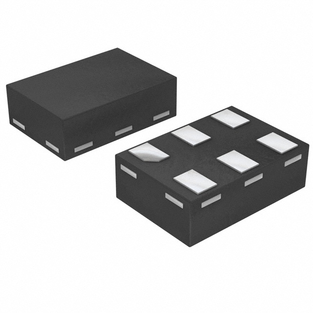
The 74AUP1G126FW5-7 is available in a small form factor package, such as SOT-353 or DFN1010-6.
Essence
The essence of this product lies in its ability to provide efficient signal switching and amplification while consuming minimal power.
Packaging/Quantity
The 74AUP1G126FW5-7 is typically packaged in reels or tubes, with quantities varying based on customer requirements.
Specifications
- Supply Voltage Range: 0.8V to 3.6V
- Input Voltage Range: -0.5V to VCC + 0.5V
- Output Voltage Range: -0.5V to VCC + 0.5V
- Operating Temperature Range: -40°C to +85°C
- Maximum Power Dissipation: 150mW
Detailed Pin Configuration
The 74AUP1G126FW5-7 has the following pin configuration:
____
   Y1 |    | VCC
   A1 |    | Y2
  GND |____| A2
Functional Features
- Single gate buffer with output enable
- High-speed operation allows for quick signal switching
- Low power consumption makes it suitable for battery-powered devices
- Wide operating voltage range enables compatibility with various systems
Advantages and Disadvantages
Advantages
- Low power consumption extends battery life in portable devices
- High-speed operation ensures efficient signal processing
- Small package size saves board space in compact designs
Disadvantages
- Limited output current capacity may restrict use in high-power applications
- Sensitivity to electrostatic discharge (ESD) requires proper handling during assembly and usage
Working Principles
The 74AUP1G126FW5-7 operates as a single gate buffer with an output enable feature. It amplifies and switches input signals based on the control input, providing a buffered output signal. The low power consumption and high-speed operation are achieved through advanced semiconductor technology.
Detailed Application Field Plans
The 74AUP1G126FW5-7 finds applications in various electronic systems, including but not limited to: - Mobile phones - Tablets - Portable media players - Wearable devices - IoT (Internet of Things) devices
Detailed and Complete Alternative Models
Some alternative models that offer similar functionality to the 74AUP1G126FW5-7 include: - SN74LVC1G126DBVR - MC74VHC1G126DTT1G - TC7SZ126FU
These alternatives can be considered based on specific project requirements and availability.
In conclusion, the 74AUP1G126FW5-7 is a versatile integrated circuit used for signal switching and amplification. Its low power consumption, high-speed operation, and small package size make it suitable for a wide range of electronic devices. However, its limited output current capacity and sensitivity to ESD should be taken into consideration during design and implementation.
技術ソリューションにおける 74AUP1G126FW5-7 の適用に関連する 10 件の一般的な質問と回答をリストします。
Sure! Here are 10 common questions and answers related to the application of 74AUP1G126FW5-7 in technical solutions:
Q1: What is the 74AUP1G126FW5-7? A1: The 74AUP1G126FW5-7 is a single bus buffer gate with 3-state output, designed for low-power applications.
Q2: What is the operating voltage range of the 74AUP1G126FW5-7? A2: The operating voltage range is from 0.8V to 3.6V.
Q3: What is the maximum output current of the 74AUP1G126FW5-7? A3: The maximum output current is 32mA.
Q4: Can the 74AUP1G126FW5-7 be used as a level shifter? A4: Yes, the 74AUP1G126FW5-7 can be used as a level shifter due to its wide operating voltage range.
Q5: What is the propagation delay of the 74AUP1G126FW5-7? A5: The propagation delay is typically 2.5ns.
Q6: Can the 74AUP1G126FW5-7 drive capacitive loads? A6: Yes, the 74AUP1G126FW5-7 can drive capacitive loads up to 50pF.
Q7: Is the 74AUP1G126FW5-7 compatible with other logic families? A7: Yes, the 74AUP1G126FW5-7 is compatible with both CMOS and TTL logic families.
Q8: Can the 74AUP1G126FW5-7 be used in battery-powered applications? A8: Yes, the 74AUP1G126FW5-7 is suitable for battery-powered applications due to its low-power design.
Q9: What is the package type of the 74AUP1G126FW5-7? A9: The 74AUP1G126FW5-7 is available in a small SOT353 package.
Q10: Can the 74AUP1G126FW5-7 be used in high-speed applications? A10: No, the 74AUP1G126FW5-7 is not recommended for high-speed applications as it has a relatively slow propagation delay.
Please note that these answers are based on general information about the 74AUP1G126FW5-7 and may vary depending on specific application requirements.