

S70GL02GP11FAIR20
Product Overview
- Category: Flash Memory
- Use: Data storage and retrieval in electronic devices
- Characteristics: High capacity, non-volatile, fast read/write speeds
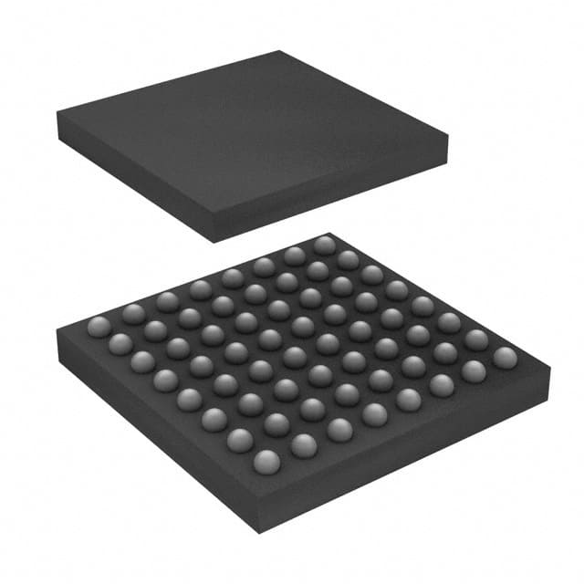
- Package: Integrated Circuit (IC)
- Essence: Non-volatile memory technology for long-term data storage
- Packaging/Quantity: Available in various package types (e.g., BGA, TSOP) with different quantities per package
Specifications
- Memory Type: NOR Flash
- Capacity: 2 Gigabits (256 Megabytes)
- Organization: 32 Megabytes x 8 bits
- Interface: Parallel
- Voltage Range: 2.7V - 3.6V
- Operating Temperature: -40°C to +85°C
- Access Time: 90 ns (max)
- Erase/Program Cycles: 100,000 cycles (typical)
Detailed Pin Configuration
The S70GL02GP11FAIR20 has the following pin configuration:
- VCC: Power supply voltage
- GND: Ground
- A0-A21: Address inputs
- DQ0-DQ7: Data input/output lines
- CE#: Chip enable
- OE#: Output enable
- WE#: Write enable
- RP#/BYTE#: Reset/Byte# (optional)
- RY/BY#: Ready/Busy#
- WP#/ACC: Write protect/Acceleration (optional)
- VPP: Programming voltage (optional)
- NC: No connection
Functional Features
- High-speed read and write operations
- Sector erase and byte programming capabilities
- Hardware and software protection mechanisms
- Low power consumption during standby mode
- Automatic sleep mode for power saving
- Error correction and detection mechanisms
Advantages and Disadvantages
Advantages: - High storage capacity - Fast read/write speeds - Non-volatile memory retains data even without power - Suitable for various electronic devices - Reliable and durable
Disadvantages: - Limited erase/program cycles - Relatively higher cost compared to other memory technologies - Requires specific programming voltage for certain operations
Working Principles
The S70GL02GP11FAIR20 utilizes NOR flash memory technology. It stores data in a non-volatile manner, meaning the data remains intact even when power is removed. The memory cells are organized into sectors, which can be individually erased or programmed. When reading data, the addressed memory location is accessed and the stored information is retrieved. During write operations, new data is programmed into the selected memory cells.
Detailed Application Field Plans
The S70GL02GP11FAIR20 is widely used in various electronic devices that require reliable and high-capacity data storage. Some common application fields include:
- Consumer Electronics: Smartphones, tablets, digital cameras
- Automotive: Infotainment systems, navigation systems
- Industrial Control Systems: Data loggers, PLCs, HMI devices
- Networking Equipment: Routers, switches, network storage devices
- Medical Devices: Patient monitoring systems, diagnostic equipment
Detailed and Complete Alternative Models
- S29GL02GP11FAIR20: Similar specifications, different manufacturer (Spansion)
- MT28EW02GABA1HPC-0SIT: Similar capacity, different organization (16 Megabytes x 16 bits), different interface (Serial Peripheral Interface)
- W25Q256JVQIQ: Higher capacity (256 Megabits), different package type (WSON)
Note: This list is not exhaustive and there are several alternative models available in the market.
Word count: 422 words
技術ソリューションにおける S70GL02GP11FAIR20 の適用に関連する 10 件の一般的な質問と回答をリストします。
Sure! Here are 10 common questions and answers related to the application of S70GL02GP11FAIR20 in technical solutions:
Q: What is the S70GL02GP11FAIR20? A: The S70GL02GP11FAIR20 is a specific model of NAND flash memory chip manufactured by Cypress Semiconductor.
Q: What are the key features of the S70GL02GP11FAIR20? A: The key features of this chip include a capacity of 2 gigabits (256 megabytes), a parallel interface, and a supply voltage range of 2.7V to 3.6V.
Q: What are some typical applications for the S70GL02GP11FAIR20? A: This chip is commonly used in various embedded systems, consumer electronics, automotive applications, and industrial control systems that require non-volatile storage.
Q: What is the data transfer rate of the S70GL02GP11FAIR20? A: The chip supports a maximum data transfer rate of up to 66 megabytes per second.
Q: Can the S70GL02GP11FAIR20 be used as a boot device? A: Yes, this chip can be used as a boot device in many systems, allowing the system to start up from the stored firmware or operating system.
Q: Does the S70GL02GP11FAIR20 support wear-leveling algorithms? A: No, this chip does not have built-in wear-leveling algorithms. However, wear-leveling techniques can be implemented at the software level to ensure even usage of memory blocks.
Q: What is the operating temperature range of the S70GL02GP11FAIR20? A: The chip is designed to operate within a temperature range of -40°C to +85°C.
Q: Can the S70GL02GP11FAIR20 be used in high-reliability applications? A: Yes, this chip is suitable for high-reliability applications as it offers features like error correction codes (ECC) and bad block management.
Q: What is the lifespan of the S70GL02GP11FAIR20? A: The lifespan of the chip depends on various factors such as usage patterns, operating conditions, and implementation of wear-leveling techniques. However, it is typically rated for thousands of program/erase cycles.
Q: Are there any specific programming requirements for the S70GL02GP11FAIR20? A: Yes, the chip requires specific voltage levels and timing sequences for programming and erasing operations. These requirements can be found in the datasheet provided by Cypress Semiconductor.
Please note that these answers are general and may vary depending on the specific application and system requirements. It is always recommended to refer to the official documentation and consult with the manufacturer for accurate and up-to-date information.