

CY7C4225V-15ASXC
Product Overview
Category
The CY7C4225V-15ASXC belongs to the category of integrated circuits (ICs), specifically a synchronous dual-port static random access memory (SDP SRAM) chip.
Use
This IC is primarily used in applications that require high-speed and reliable data storage and retrieval. It is commonly employed in networking equipment, telecommunications systems, and other devices that demand efficient data buffering and caching capabilities.
Characteristics
- Synchronous operation: The CY7C4225V-15ASXC operates synchronously with the system clock, ensuring precise timing and data integrity.
- Dual-port architecture: This chip features two independent ports, allowing simultaneous read and write operations from different sources.
- High-speed performance: With a maximum operating frequency of 150 MHz, this IC offers rapid data transfer rates, enabling efficient real-time processing.
- Low power consumption: The CY7C4225V-15ASXC is designed to minimize power usage, making it suitable for battery-powered devices.
- Wide voltage range: It supports a broad supply voltage range, enhancing compatibility with various system configurations.
Package and Quantity
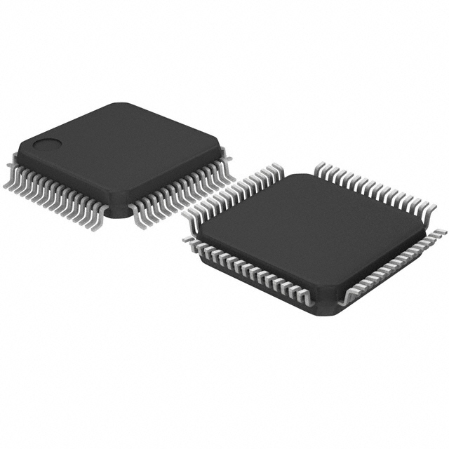
The CY7C4225V-15ASXC is available in a small-outline integrated circuit (SOIC) package. Each package contains one IC.
Specifications
- Memory capacity: 4 megabits (512 kilobytes)
- Organization: 256K x 16 bits
- Access time: 15 ns
- Operating voltage: 3.3V
- Operating temperature range: -40°C to +85°C
- Pin count: 48
Detailed Pin Configuration
The CY7C4225V-15ASXC has a total of 48 pins, which are assigned specific functions. Here is a detailed pin configuration:
- VCCQ: Power supply for I/O circuitry
- VCC: Power supply for core logic
- GND: Ground reference
- A0-A17: Address inputs
- DQ0-DQ15: Data input/output pins
- WE: Write enable
- OE: Output enable
- UB/LB: Upper byte/lower byte control
- CE1, CE2: Chip enable inputs
- CLK: System clock input
- BYTE: Byte write enable
- RST: Reset input
- INTA, INTB: Interrupt request outputs
- BUSY: Busy output
- ADSC: Address status change output
Functional Features
Simultaneous Read and Write Operations
The CY7C4225V-15ASXC allows independent read and write operations to occur simultaneously on its dual ports. This feature enables efficient data transfer between different sources without any conflicts.
Synchronous Operation
By synchronizing its operation with the system clock, this IC ensures accurate timing and reliable data transfer. The synchronous nature of the CY7C4225V-15ASXC minimizes the risk of data corruption or loss.
High-Speed Performance
With a maximum operating frequency of 150 MHz, this IC offers fast data access times, enabling high-speed data processing. It is well-suited for applications that require real-time data handling.
Low Power Consumption
The CY7C4225V-15ASXC is designed to consume minimal power, making it suitable for energy-efficient devices and battery-powered applications. Its low power consumption helps prolong battery life and reduces overall power usage.
Advantages and Disadvantages
Advantages
- Dual-port architecture allows simultaneous read and write operations.
- High-speed performance enables efficient real-time data processing.
- Low power consumption makes it suitable for battery-powered devices.
- Wide voltage range enhances compatibility with different system configurations.
Disadvantages
- Limited memory capacity (4 megabits) compared to newer SRAM chips.
- Access time of 15 ns may not meet the requirements of certain high-performance applications.
Working Principles
The CY7C4225V-15ASXC operates based on static random access memory (SRAM) principles. It stores data in a volatile manner, meaning that the stored information is lost when power is removed. The chip utilizes a dual-port architecture, allowing simultaneous read and write operations from different sources. Synchronous operation ensures precise timing and reliable data transfer.
Detailed Application Field Plans
The CY7C4225V-15ASXC finds application in various fields that require high-speed data storage and retrieval capabilities. Some specific application areas include:
- Networking Equipment: This IC can be used in routers, switches, and network interface cards to provide efficient data buffering and caching, enhancing overall network performance.
- Telecommunications Systems: In telecommunications infrastructure, the CY7C4225V-15ASXC can be utilized for buffering and storing voice and data packets, ensuring smooth
技術ソリューションにおける CY7C4225V-15ASXC の適用に関連する 10 件の一般的な質問と回答をリストします。
Sure! Here are 10 common questions and answers related to the application of CY7C4225V-15ASXC in technical solutions:
Question: What is the maximum operating frequency of CY7C4225V-15ASXC?
Answer: The maximum operating frequency of CY7C4225V-15ASXC is 133 MHz.Question: What is the voltage supply range for CY7C4225V-15ASXC?
Answer: The voltage supply range for CY7C4225V-15ASXC is 3.0V to 3.6V.Question: Can CY7C4225V-15ASXC be used in industrial applications?
Answer: Yes, CY7C4225V-15ASXC is suitable for industrial applications due to its wide temperature range and robust design.Question: How many I/O pins does CY7C4225V-15ASXC have?
Answer: CY7C4225V-15ASXC has a total of 36 I/O pins.Question: Is CY7C4225V-15ASXC compatible with other microcontrollers or processors?
Answer: Yes, CY7C4225V-15ASXC is compatible with various microcontrollers and processors that support the SRAM interface.Question: What is the typical access time of CY7C4225V-15ASXC?
Answer: The typical access time of CY7C4225V-15ASXC is 15 ns.Question: Can CY7C4225V-15ASXC be used in battery-powered devices?
Answer: Yes, CY7C4225V-15ASXC can be used in battery-powered devices as it operates at low power consumption.Question: Does CY7C4225V-15ASXC support burst mode operation?
Answer: Yes, CY7C4225V-15ASXC supports burst mode operation for efficient data transfer.Question: What is the capacity of CY7C4225V-15ASXC?
Answer: CY7C4225V-15ASXC has a capacity of 256K (32K x 8) bits.Question: Is CY7C4225V-15ASXC RoHS compliant?
Answer: Yes, CY7C4225V-15ASXC is RoHS compliant, ensuring it meets environmental regulations.
Please note that these answers are based on general information and it's always recommended to refer to the datasheet or consult the manufacturer for specific details and application requirements.