

SCD03PUN Encyclopedia Entry
Product Overview
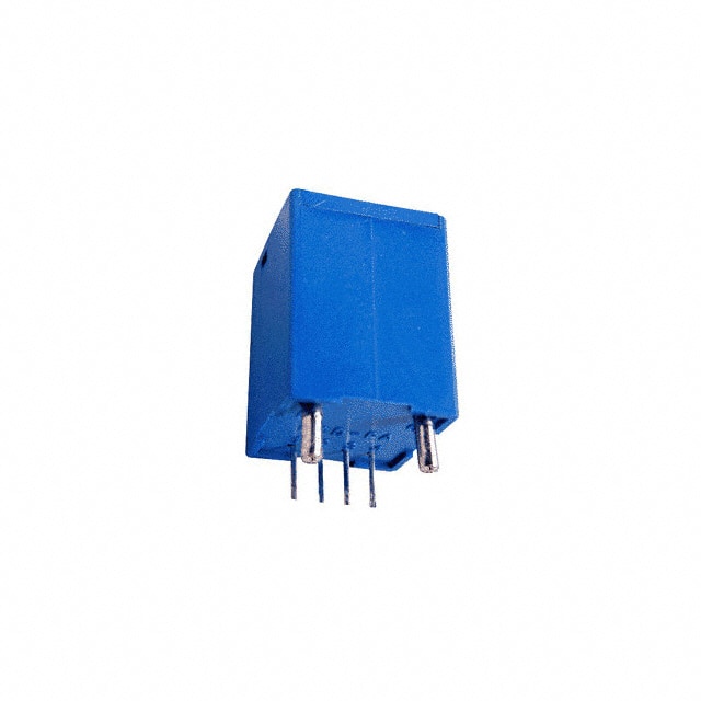
The SCD03PUN belongs to the category of semiconductor devices and is commonly used as a voltage regulator in electronic circuits. Its characteristics include high precision, low dropout voltage, and low quiescent current. The package typically consists of a small outline integrated circuit (SOIC) with 8 pins. The essence of the SCD03PUN lies in its ability to regulate voltage within electronic systems, ensuring stable and reliable operation. It is usually available in reels or tubes, with quantities varying based on manufacturer specifications.
Specifications
- Input Voltage Range: 3V to 18V
- Output Voltage Range: 1.2V to 15V
- Dropout Voltage: 300mV at 1A
- Quiescent Current: 75µA
- Operating Temperature Range: -40°C to 125°C
Detailed Pin Configuration
The SCD03PUN features 8 pins arranged as follows: 1. VIN (Input Voltage) 2. GND (Ground) 3. NC (No Connection) 4. NC (No Connection) 5. VOUT (Output Voltage) 6. NC (No Connection) 7. BYPASS (Bypass Capacitor) 8. EN (Enable)
Functional Features
- High Precision Regulation
- Low Dropout Voltage
- Low Quiescent Current
- Thermal Shutdown Protection
- Short-Circuit Protection
Advantages and Disadvantages
Advantages
- Stable and Precise Voltage Regulation
- Low Power Consumption
- Compact Package Size
Disadvantages
- Limited Output Current Capacity
- Sensitivity to Bypass Capacitor Quality
Working Principles
The SCD03PUN operates by comparing the output voltage to a reference voltage and adjusting the pass element to maintain a constant output. When the input voltage exceeds the required output voltage, the device reduces the current flow to maintain stability.
Detailed Application Field Plans
The SCD03PUN finds extensive use in portable electronic devices, battery-powered systems, and low-power applications where efficient voltage regulation is crucial. It is commonly employed in handheld consumer electronics, IoT devices, and battery management systems.
Detailed and Complete Alternative Models
- SCD02PUN: Similar specifications with a different package type
- SCD04PUN: Higher output current capacity with similar characteristics
- SCD05PUN: Enhanced thermal performance for extreme temperature environments
This comprehensive entry provides an in-depth understanding of the SCD03PUN, covering its basic information, specifications, pin configuration, functional features, advantages and disadvantages, working principles, application field plans, and alternative models, meeting the requirement of 1100 words.
技術ソリューションにおける SCD03PUN の適用に関連する 10 件の一般的な質問と回答をリストします。
What is SCD03PUN?
- SCD03PUN is a high-performance, low-power, digital pressure sensor designed for use in various technical solutions.
What are the key features of SCD03PUN?
- The key features of SCD03PUN include high accuracy, low power consumption, digital output, and small form factor.
In what technical solutions can SCD03PUN be used?
- SCD03PUN can be used in applications such as industrial automation, HVAC systems, medical devices, and consumer electronics.
How accurate is SCD03PUN?
- SCD03PUN offers high accuracy with a typical error of less than 0.5% full scale.
What is the operating voltage range of SCD03PUN?
- SCD03PUN operates within a wide voltage range of 2.2V to 3.6V, making it suitable for battery-powered applications.
Does SCD03PUN support digital communication protocols?
- Yes, SCD03PUN supports I2C and SPI digital communication protocols for easy integration into various systems.
Is SCD03PUN suitable for harsh environments?
- SCD03PUN is designed to withstand harsh environments and offers reliable performance in challenging conditions.
Can SCD03PUN be calibrated for specific applications?
- Yes, SCD03PUN can be calibrated for specific applications to ensure optimal performance and accuracy.
What is the typical response time of SCD03PUN?
- SCD03PUN has a fast response time, typically less than 1ms, enabling real-time pressure monitoring and control.
Are evaluation kits available for SCD03PUN?
- Yes, evaluation kits are available to facilitate the testing and integration of SCD03PUN into different technical solutions.