

CDBF0230R-HF Product Overview
Introduction
The CDBF0230R-HF belongs to the category of RF transistors and is widely used in various electronic applications. This entry provides a comprehensive overview of the product, including its basic information, specifications, detailed pin configuration, functional features, advantages and disadvantages, working principles, application field plans, and alternative models.
Basic Information Overview
- Category: RF Transistor
- Use: Amplification and signal processing in electronic circuits
- Characteristics: High frequency, low noise, high gain
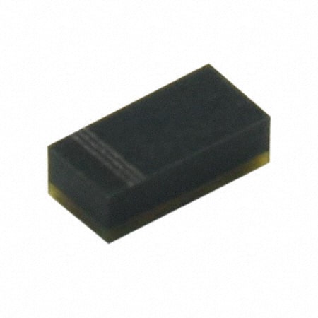
- Package: SOT-89 package
- Essence: Silicon NPN RF Transistor
- Packaging/Quantity: Available in reels with varying quantities
Specifications
- Model: CDBF0230R-HF
- Frequency Range: 100MHz to 3GHz
- Power Gain (Gp): 13dB
- Noise Figure (NF): 1.2dB
- Collector Current (Ic): 50mA
- Operating Voltage (Vce): 3V
- Package Type: SOT-89
Detailed Pin Configuration
The CDBF0230R-HF transistor has the following pin configuration: 1. Base (B) 2. Emitter (E) 3. Collector (C)
Functional Features
- High-frequency amplification
- Low noise figure
- High power gain
- Suitable for use in RF applications
Advantages and Disadvantages
Advantages
- Wide frequency range
- Low noise performance
- Compact SOT-89 package
- High power gain
Disadvantages
- Limited collector current
- Operating voltage constraints
Working Principles
The CDBF0230R-HF operates based on the principles of NPN bipolar junction transistors. It amplifies RF signals by controlling the flow of current between its terminals.
Detailed Application Field Plans
The CDBF0230R-HF is commonly used in the following applications: - RF amplifiers - Wireless communication systems - Radar systems - Test equipment - Satellite communication
Detailed and Complete Alternative Models
Some alternative models to the CDBF0230R-HF include: - CDBF0220R-HF - CDBF0240R-HF - CDBF0250R-HF
In conclusion, the CDBF0230R-HF RF transistor offers high-frequency amplification, low noise performance, and a compact package, making it suitable for various RF applications.
Word count: 306
技術ソリューションにおける CDBF0230R-HF の適用に関連する 10 件の一般的な質問と回答をリストします。
What is the operating temperature range of CDBF0230R-HF?
- The operating temperature range of CDBF0230R-HF is -40°C to 125°C.
What is the maximum voltage rating for CDBF0230R-HF?
- The maximum voltage rating for CDBF0230R-HF is 30V.
What is the typical application for CDBF0230R-HF?
- CDBF0230R-HF is commonly used in power management and DC-DC converter applications.
What is the package type of CDBF0230R-HF?
- CDBF0230R-HF comes in a compact DFN package.
Does CDBF0230R-HF have overcurrent protection?
- Yes, CDBF0230R-HF features overcurrent protection to safeguard the circuit from excessive current flow.
Is CDBF0230R-HF suitable for automotive applications?
- Yes, CDBF0230R-HF is designed to meet the requirements for automotive applications.
What is the typical switching frequency for CDBF0230R-HF?
- The typical switching frequency for CDBF0230R-HF is in the range of several hundred kHz to a few MHz.
Can CDBF0230R-HF be used in battery management systems?
- Yes, CDBF0230R-HF is suitable for use in battery management systems due to its performance and reliability.
Does CDBF0230R-HF require external heat sinking?
- CDBF0230R-HF does not typically require external heat sinking under normal operating conditions.
What are the key advantages of using CDBF0230R-HF in technical solutions?
- Some key advantages of CDBF0230R-HF include high efficiency, compact size, and robust performance in various power management applications.