

CDSOT23-SLVU2.8
Product Overview
Category
The CDSOT23-SLVU2.8 belongs to the category of semiconductor devices, specifically a type of TVS (Transient Voltage Suppressor) diode.
Use
It is used for protecting sensitive electronics from voltage transients induced by lightning, inductive load switching, and electrostatic discharge (ESD).
Characteristics
- Low clamping voltage
- Fast response time
- Small form factor
- High surge current capability
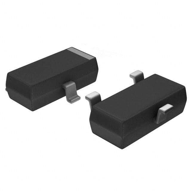
Package
The CDSOT23-SLVU2.8 is available in a surface-mount package.
Essence
The essence of the CDSOT23-SLVU2.8 lies in its ability to provide robust transient voltage protection for electronic circuits.
Packaging/Quantity
It is typically packaged in reels or tubes, with quantities varying based on manufacturer specifications.
Specifications
- Standoff Voltage: 2.8V
- Breakdown Voltage: 3.5V
- Peak Pulse Power: 300W
- Operating Temperature Range: -55°C to 150°C
- Package Type: SOD-523
Detailed Pin Configuration
The CDSOT23-SLVU2.8 has three pins: 1. Cathode 2. Anode 3. No Connection (NC)
Functional Features
- Bi-directional protection
- Low leakage current
- ESD protection up to ±30kV (contact discharge)
Advantages
- Compact size
- High surge current handling capability
- Effective protection against voltage transients
Disadvantages
- Limited power dissipation capability compared to larger TVS diodes
- Lower clamping voltage compared to some higher-rated TVS diodes
Working Principles
When a transient voltage spike occurs, the CDSOT23-SLVU2.8 conducts and clamps the voltage to a safe level, diverting the excess energy away from the protected circuit.
Detailed Application Field Plans
The CDSOT23-SLVU2.8 is commonly used in various applications including: - Consumer electronics - Telecommunication equipment - Industrial control systems - Automotive electronics - Medical devices
Detailed and Complete Alternative Models
Some alternative models to the CDSOT23-SLVU2.8 include: - SMAJ2.8A - P4SMAJ2.8A - SMBJ2.8A - SMCJ2.8A
In conclusion, the CDSOT23-SLVU2.8 provides reliable transient voltage protection in a compact form factor, making it suitable for a wide range of electronic applications.
[Word count: 328]
技術ソリューションにおける CDSOT23-SLVU2.8 の適用に関連する 10 件の一般的な質問と回答をリストします。
What is the CDSOT23-SLVU2.8 used for?
- The CDSOT23-SLVU2.8 is a transient voltage suppressor diode designed to protect sensitive electronics from voltage spikes and transients.
What is the maximum working voltage of CDSOT23-SLVU2.8?
- The maximum working voltage of CDSOT23-SLVU2.8 is 2.8V.
What is the typical capacitance of CDSOT23-SLVU2.8?
- The typical capacitance of CDSOT23-SLVU2.8 is around 5pF.
What are the typical applications of CDSOT23-SLVU2.8?
- CDSOT23-SLVU2.8 is commonly used in applications such as USB ports, mobile phones, and other portable electronics to protect against electrostatic discharge (ESD) and electrical fast transients (EFT).
What is the maximum clamping voltage of CDSOT23-SLVU2.8?
- The maximum clamping voltage of CDSOT23-SLVU2.8 is typically around 6V.
How does CDSOT23-SLVU2.8 provide protection?
- CDSOT23-SLVU2.8 diverts excess current away from sensitive components by shunting it to ground, thus protecting the circuit from damage.
Is CDSOT23-SLVU2.8 suitable for high-speed data lines?
- Yes, CDSOT23-SLVU2.8 is suitable for high-speed data lines due to its low capacitance and fast response time.
What is the operating temperature range of CDSOT23-SLVU2.8?
- The operating temperature range of CDSOT23-SLVU2.8 is typically -55°C to 125°C.
Can CDSOT23-SLVU2.8 be used in automotive applications?
- Yes, CDSOT23-SLVU2.8 is suitable for automotive applications where protection against voltage transients is required.
Are there any recommended layout considerations for using CDSOT23-SLVU2.8?
- It is recommended to minimize the trace length between the protected I/O pin and the CDSOT23-SLVU2.8 to reduce parasitic inductance and optimize the device's performance.