

ADP5061ACBZ-4-R7
Product Overview
Category
ADP5061ACBZ-4-R7 belongs to the category of integrated circuits (ICs).
Use
This product is commonly used in electronic devices for power management purposes.
Characteristics
- Integrated circuit
- Power management functionality
- Small form factor
- High efficiency
- Low power consumption
Package
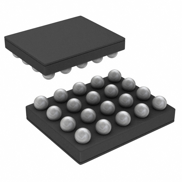
ADP5061ACBZ-4-R7 is available in a compact package, suitable for surface mount technology (SMT) assembly.
Essence
The essence of ADP5061ACBZ-4-R7 lies in its ability to efficiently manage power in electronic devices, ensuring optimal performance and energy conservation.
Packaging/Quantity
This product is typically packaged in reels or tubes, with a quantity of 2500 units per reel/tube.
Specifications
- Input voltage range: 2.7V to 5.5V
- Output voltage range: Adjustable from 0.8V to 5.2V
- Maximum output current: 3A
- Operating temperature range: -40°C to 85°C
- Package type: 20-Lead LFCSP
Detailed Pin Configuration
- VIN: Input voltage pin
- GND: Ground pin
- VOUT: Output voltage pin
- EN: Enable pin
- PGND: Power ground pin
- BST: Boost converter input pin
- SW: Switching node pin
- FB: Feedback pin
- SS: Soft-start pin
- PGOOD: Power good indicator pin
- ISET: Current limit set pin
- VREF: Reference voltage pin
- AGND: Analog ground pin
- INTVCC: Internal voltage regulator input pin
- VCC: Supply voltage pin
- PGND: Power ground pin
- PGND: Power ground pin
- PGND: Power ground pin
- PGND: Power ground pin
- PGND: Power ground pin
Functional Features
- Integrated boost converter and LDO regulator
- Wide input voltage range for compatibility with various power sources
- Adjustable output voltage to meet specific device requirements
- Current limit protection for safe operation
- Soft-start feature to minimize inrush current
- Power good indicator for system monitoring
- Internal voltage regulator for stable operation
Advantages and Disadvantages
Advantages
- Efficient power management
- Compact size
- Wide input voltage range
- Adjustable output voltage
- Comprehensive protection features
Disadvantages
- Limited maximum output current (3A)
- Operating temperature range may not be suitable for extreme environments
Working Principles
ADP5061ACBZ-4-R7 operates by converting the input voltage to a higher or lower level as required, using its integrated boost converter and LDO regulator. The output voltage can be adjusted through the feedback pin, allowing customization for different devices. The IC also incorporates various protection mechanisms to ensure safe and reliable operation.
Detailed Application Field Plans
ADP5061ACBZ-4-R7 finds applications in a wide range of electronic devices, including but not limited to: - Mobile phones - Tablets - Portable gaming consoles - Wearable devices - IoT devices - Industrial equipment
Detailed and Complete Alternative Models
- ADP5062ACBZ-4-R7
- ADP5063ACBZ-4-R7
- ADP5064ACBZ-4-R7
- ADP5065ACBZ-4-R7
- ADP5066ACBZ-4-R7
These alternative models offer similar power management functionality and can be considered as alternatives to ADP5061ACBZ-4-R7 based on specific requirements.
In conclusion, ADP5061ACBZ-4-R7 is a versatile integrated circuit designed for efficient power management in electronic devices. Its compact size, wide input voltage range, and adjustable output voltage make it suitable for various applications. While it has limitations in terms of maximum output current and operating temperature range, it offers comprehensive protection features for safe operation.
技術ソリューションにおける ADP5061ACBZ-4-R7 の適用に関連する 10 件の一般的な質問と回答をリストします。
Sure! Here are 10 common questions and answers related to the application of ADP5061ACBZ-4-R7 in technical solutions:
Q1: What is the ADP5061ACBZ-4-R7? A1: The ADP5061ACBZ-4-R7 is a power management IC (PMIC) designed for use in portable devices, such as smartphones, tablets, and wearables.
Q2: What are the key features of the ADP5061ACBZ-4-R7? A2: Some key features of the ADP5061ACBZ-4-R7 include multiple buck converters, a boost converter, a linear regulator, battery charger, and a fuel gauge.
Q3: How many buck converters are there in the ADP5061ACBZ-4-R7? A3: The ADP5061ACBZ-4-R7 has three integrated buck converters, which can be used to power different components of the system.
Q4: Can the ADP5061ACBZ-4-R7 charge multiple batteries simultaneously? A4: Yes, the ADP5061ACBZ-4-R7 supports multi-cell battery charging, allowing it to charge multiple batteries at the same time.
Q5: Does the ADP5061ACBZ-4-R7 have any protection features? A5: Yes, the ADP5061ACBZ-4-R7 includes various protection features like overvoltage protection, overcurrent protection, and thermal shutdown to ensure safe operation.
Q6: What is the input voltage range supported by the ADP5061ACBZ-4-R7? A6: The ADP5061ACBZ-4-R7 supports an input voltage range of 2.8V to 6.5V, making it compatible with a wide range of power sources.
Q7: Can the ADP5061ACBZ-4-R7 be controlled through an external microcontroller? A7: Yes, the ADP5061ACBZ-4-R7 can be controlled and monitored using an external microcontroller via its I2C interface.
Q8: What is the purpose of the fuel gauge in the ADP5061ACBZ-4-R7? A8: The fuel gauge in the ADP5061ACBZ-4-R7 provides accurate estimation of the battery's state of charge, allowing for better battery management.
Q9: Is the ADP5061ACBZ-4-R7 suitable for low-power applications? A9: Yes, the ADP5061ACBZ-4-R7 is designed to operate efficiently in low-power applications, helping to extend battery life.
Q10: Are there any evaluation boards available for the ADP5061ACBZ-4-R7? A10: Yes, Analog Devices offers an evaluation board for the ADP5061ACBZ-4-R7, which allows users to test and evaluate its performance in their specific applications.
Please note that these answers are general and may vary depending on the specific requirements and use cases of your technical solution.