

ADN2813ACPZ-RL7
Overview
Category
ADN2813ACPZ-RL7 belongs to the category of integrated circuits (ICs).
Use
It is commonly used in electronic devices for signal processing and data communication.
Characteristics
- High-speed performance
- Low power consumption
- Compact size
- Reliable operation
Package
ADN2813ACPZ-RL7 is available in a small form factor package, which ensures easy integration into various electronic systems.
Essence
The essence of ADN2813ACPZ-RL7 lies in its ability to process signals efficiently and accurately, enabling reliable data transmission.
Packaging/Quantity
This product is typically packaged in reels or trays, with a quantity of 2500 units per reel/tray.
Specifications and Parameters
- Input Voltage Range: 2.5V - 3.3V
- Operating Temperature Range: -40°C to +85°C
- Data Rate: Up to 2.5 Gbps
- Power Supply: 3.3V
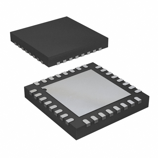
- Package Type: LFCSP
- Pin Count: 32
Pin Configuration
For detailed and complete pin configuration information, please refer to the datasheet provided by the manufacturer.
Functional Characteristics
ADN2813ACPZ-RL7 offers the following functional characteristics:
- Signal amplification
- Clock recovery
- Equalization
- Error detection and correction
Advantages and Disadvantages
Advantages
- High-speed performance enables efficient data transmission
- Low power consumption helps conserve energy
- Compact size allows for easy integration into various electronic systems
- Reliable operation ensures stable signal processing
Disadvantages
- Limited compatibility with certain operating voltages
- May require additional components for specific applications
Applicable Range of Products
ADN2813ACPZ-RL7 is suitable for use in a wide range of products, including:
- Optical transceivers
- Network switches
- Data communication equipment
Working Principles
ADN2813ACPZ-RL7 operates based on advanced signal processing algorithms and integrated circuit design. It receives input signals, amplifies them, performs clock recovery, equalizes the data, and detects/corrects errors to ensure accurate transmission.
Detailed Application Field Plans
ADN2813ACPZ-RL7 can be applied in various fields, such as:
- Telecommunications: Used in optical network equipment for high-speed data transmission.
- Data Centers: Integrated into network switches for efficient data processing.
- Broadcast Systems: Enables reliable signal transmission in broadcasting applications.
Detailed Alternative Models
Some alternative models to ADN2813ACPZ-RL7 include:
- ADN2814ACPZ-RL7
- ADN2815ACPZ-RL7
- ADN2816ACPZ-RL7
Please refer to the manufacturer's documentation for detailed specifications of these alternative models.
5 Common Technical Questions and Answers
Q: What is the maximum data rate supported by ADN2813ACPZ-RL7? A: ADN2813ACPZ-RL7 supports data rates up to 2.5 Gbps.
Q: Can ADN2813ACPZ-RL7 operate with a voltage lower than 2.5V? A: No, the recommended input voltage range for ADN2813ACPZ-RL7 is 2.5V - 3.3V.
Q: Does ADN2813ACPZ-RL7 require external components for clock recovery? A: No, ADN2813ACPZ-RL7 has built-in clock recovery functionality.
Q: What is the operating temperature range of ADN2813ACPZ-RL7? A: ADN2813ACPZ-RL7 can operate within a temperature range of -40°C to +85°C.
Q: How many pins does ADN2813ACPZ-RL7 have? A: ADN2813ACPZ-RL7 has a total of 32 pins.
This concludes the encyclopedia entry for ADN2813ACPZ-RL7, providing an overview of its category, use, characteristics, package, specifications, pin configuration, functional characteristics, advantages and disadvantages, applicable range of products, working principles, detailed application field plans, alternative models, and common technical questions and answers.