

ADCMP563BCPZ-R2
Product Overview
Category: Analog-to-Digital Converter (ADC)
Use: The ADCMP563BCPZ-R2 is a high-speed, low-power, 12-bit analog-to-digital converter designed for various applications in the field of electronics. It converts continuous analog signals into discrete digital values, enabling accurate and reliable data acquisition.
Characteristics: - High-speed conversion with a sampling rate of up to 100 Mega Samples Per Second (MSPS) - Low power consumption, making it suitable for battery-powered devices - 12-bit resolution provides precise digital representation of analog signals - Wide input voltage range allows for versatile signal processing - Small package size (CPZ) ensures space-efficient integration into electronic systems
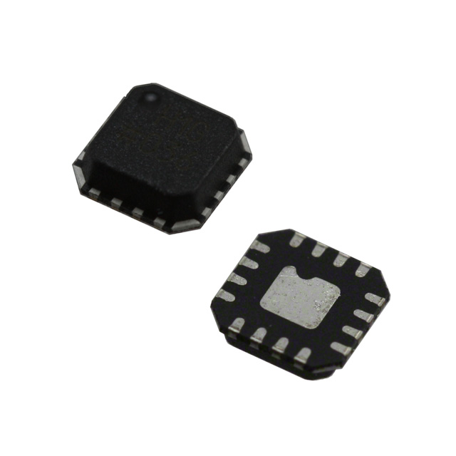
Package: The ADCMP563BCPZ-R2 is available in a compact lead-free LFCSP package, which stands for Lead Frame Chip Scale Package. This package offers excellent thermal performance and ease of handling during assembly.
Essence: The essence of the ADCMP563BCPZ-R2 lies in its ability to accurately convert analog signals into digital format, facilitating further processing and analysis by digital systems.
Packaging/Quantity: The ADCMP563BCPZ-R2 is typically sold in reels or tubes, with each reel containing 2500 units.
Specifications
- Resolution: 12 bits
- Sampling Rate: Up to 100 MSPS
- Input Voltage Range: ±1 V
- Power Supply: 3.3 V
- Power Consumption: 75 mW
- Operating Temperature Range: -40°C to +85°C
Pin Configuration
The ADCMP563BCPZ-R2 features a total of 32 pins, each serving a specific purpose. Here is a detailed pin configuration:
| Pin Number | Pin Name | Function | |------------|----------|----------| | 1 | VREFP | Positive Reference Voltage Input | | 2 | VREFN | Negative Reference Voltage Input | | 3 | VIN+ | Positive Analog Input | | 4 | VIN- | Negative Analog Input | | 5 | AGND | Analog Ground | | 6 | VCM | Common Mode Voltage Output | | 7-10 | DGND | Digital Ground | | 11 | DVDD | Digital Power Supply | | 12 | CLK | Clock Input | | 13 | CS | Chip Select Input | | 14 | SDO | Serial Data Output | | 15 | SDI | Serial Data Input | | 16 | SCLK | Serial Clock Input | | 17-32 | NC | No Connection |
Functional Features
The ADCMP563BCPZ-R2 offers several functional features that enhance its performance and usability:
High-Speed Conversion: With a sampling rate of up to 100 MSPS, the ADCMP563BCPZ-R2 can accurately capture fast-changing analog signals.
Low Power Consumption: The ADC operates with a power consumption of only 75 mW, making it suitable for power-constrained applications.
Versatile Input Range: The input voltage range of ±1 V allows the ADC to handle a wide variety of analog signals.
Serial Data Interface: The ADCMP563BCPZ-R2 utilizes a serial data interface (SDI, SDO, SCLK) for easy integration with digital systems.
Advantages and Disadvantages
Advantages: - High-speed conversion enables real-time signal processing. - Low power consumption prolongs battery life in portable devices. - Wide input voltage range accommodates various signal types. - Small package size allows for space-efficient integration.
Disadvantages: - Limited resolution of 12 bits may not be sufficient for certain high-precision applications. - Requires an external clock source for operation.
Working Principles
The ADCMP563BCPZ-R2 operates based on the successive approximation method. It samples the analog input voltage and compares it to a reference voltage. By iteratively adjusting the digital code, the converter converges to a binary representation that closely matches the input voltage. This process occurs at a high speed, allowing for real-time conversion of analog signals into digital format.
Detailed Application Field Plans
The ADCMP563BCPZ-R2 finds application in various fields, including but not limited to:
Communications: The ADC can be used in wireless communication systems to digitize analog signals received from antennas or transmitted through radio frequency circuits.
Medical Devices: In medical equipment such as electrocardiographs or blood pressure monitors, the ADC enables accurate measurement and analysis of physiological signals.
Industrial Automation: The ADC is suitable for industrial control systems, where it
技術ソリューションにおける ADCMP563BCPZ-R2 の適用に関連する 10 件の一般的な質問と回答をリストします。
Sure! Here are 10 common questions and answers related to the application of ADCMP563BCPZ-R2 in technical solutions:
Q: What is the ADCMP563BCPZ-R2? A: The ADCMP563BCPZ-R2 is a high-speed comparator IC (integrated circuit) designed for use in various technical applications.
Q: What is the operating voltage range of the ADCMP563BCPZ-R2? A: The ADCMP563BCPZ-R2 operates within a voltage range of 2.7V to 5.5V.
Q: What is the maximum input voltage that the ADCMP563BCPZ-R2 can handle? A: The ADCMP563BCPZ-R2 can handle input voltages up to VDD + 0.3V.
Q: What is the typical response time of the ADCMP563BCPZ-R2? A: The typical response time of the ADCMP563BCPZ-R2 is around 6 ns.
Q: Can the ADCMP563BCPZ-R2 be used in low-power applications? A: Yes, the ADCMP563BCPZ-R2 has a low power consumption and can be used in low-power applications.
Q: Does the ADCMP563BCPZ-R2 have built-in hysteresis? A: Yes, the ADCMP563BCPZ-R2 has built-in hysteresis to improve noise immunity and stability.
Q: What is the output type of the ADCMP563BCPZ-R2? A: The ADCMP563BCPZ-R2 has an open-drain output.
Q: Can the ADCMP563BCPZ-R2 operate in harsh environments? A: The ADCMP563BCPZ-R2 has a wide operating temperature range of -40°C to +125°C, making it suitable for harsh environments.
Q: What is the input voltage range of the ADCMP563BCPZ-R2? A: The ADCMP563BCPZ-R2 has an input voltage range from VSS - 0.3V to VDD + 0.3V.
Q: Is the ADCMP563BCPZ-R2 RoHS compliant? A: Yes, the ADCMP563BCPZ-R2 is RoHS (Restriction of Hazardous Substances) compliant, ensuring it meets environmental regulations.
Please note that these answers are general and may vary depending on the specific application and requirements. It's always recommended to refer to the datasheet or consult with the manufacturer for detailed information.