

AD7840JNZ
Product Overview
Category
AD7840JNZ belongs to the category of integrated circuits (ICs).
Use
The AD7840JNZ is primarily used for analog-to-digital conversion in various electronic systems.
Characteristics
- High precision: The AD7840JNZ offers high-resolution analog-to-digital conversion, ensuring accurate measurement and control.
- Low power consumption: This IC is designed to operate with minimal power consumption, making it suitable for battery-powered devices.
- Fast conversion speed: The AD7840JNZ provides fast conversion times, enabling real-time data acquisition.
- Wide input voltage range: It can handle a wide range of input voltages, allowing for versatile applications.
- Small package size: The AD7840JNZ comes in a compact package, saving valuable board space in electronic designs.
Package
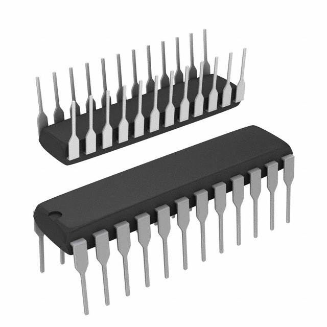
The AD7840JNZ is available in a 28-pin plastic dual in-line package (PDIP).
Essence
The essence of the AD7840JNZ lies in its ability to convert analog signals into digital data with high accuracy and speed.
Packaging/Quantity
The AD7840JNZ is typically sold in reels or tubes, with a quantity of 100 units per package.
Specifications
- Resolution: 12 bits
- Input Voltage Range: ±10V
- Conversion Time: 1.25 µs
- Operating Temperature Range: -40°C to +85°C
- Supply Voltage: +5V
- Power Consumption: 20 mW (typical)
Detailed Pin Configuration
The AD7840JNZ features the following pin configuration:
- VREF
- AGND
- DGND
- VIN
- VDD
- CS
- WR
- RD
- BUSY
- D0
- D1
- D2
- D3
- D4
- D5
- D6
- D7
- D8
- D9
- D10
- D11
- D12
- D13
- D14
- D15
- D16
- D17
- D18
Functional Features
The AD7840JNZ offers the following functional features:
- High-resolution analog-to-digital conversion
- Serial interface for easy integration with microcontrollers and other digital systems
- Internal reference voltage for accurate conversions
- Programmable input range for flexible signal handling
- Conversion start and end indicators for synchronization
Advantages and Disadvantages
Advantages
- High precision and accuracy in analog-to-digital conversion
- Low power consumption, suitable for battery-powered devices
- Fast conversion speed for real-time applications
- Wide input voltage range for versatile use cases
- Compact package size saves board space
Disadvantages
- Limited resolution compared to higher-end ADCs
- Requires external components for proper operation
- Relatively higher cost compared to lower-resolution ADCs
Working Principles
The AD7840JNZ operates based on the successive approximation register (SAR) architecture. It samples the analog input voltage, compares it to a reference voltage, and performs a binary search to determine the digital representation of the input signal.
Detailed Application Field Plans
The AD7840JNZ finds applications in various fields, including:
- Industrial automation: Used for precise measurement and control in industrial processes.
- Medical equipment: Enables accurate data acquisition in medical devices such as patient monitors.
- Test and measurement instruments: Provides high-resolution measurements in laboratory equipment.
- Communication systems: Used for signal processing and data acquisition in communication devices.
- Automotive electronics: Enables analog-to-digital conversion in automotive control systems.
Detailed and Complete Alternative Models
- AD7840JN: Similar to AD7840JNZ but comes in a different package (PDIP).
- AD7840KN: Higher temperature range variant (-40°C to +125°C) of AD7840JNZ.
- AD7841JNZ: 14-bit resolution version of AD7840JNZ.
- AD7850JNZ: Higher-resolution (16-bit) ADC with similar features to AD7840JNZ.
These alternative models offer similar functionality and can be considered based on specific application requirements.
Word count: 529 words
技術ソリューションにおける AD7840JNZ の適用に関連する 10 件の一般的な質問と回答をリストします。
Sure! Here are 10 common questions and answers related to the application of AD7840JNZ in technical solutions:
Q: What is AD7840JNZ? A: AD7840JNZ is a high-speed, low-power, 12-bit digital-to-analog converter (DAC) manufactured by Analog Devices.
Q: What is the operating voltage range of AD7840JNZ? A: The operating voltage range of AD7840JNZ is typically between +5V and +15V.
Q: What is the resolution of AD7840JNZ? A: AD7840JNZ has a resolution of 12 bits, which means it can provide 4096 different output voltage levels.
Q: What is the maximum output current of AD7840JNZ? A: The maximum output current of AD7840JNZ is typically 2 mA.
Q: Can AD7840JNZ operate in both single-ended and differential modes? A: Yes, AD7840JNZ can operate in both single-ended and differential modes, providing flexibility in various applications.
Q: What is the settling time of AD7840JNZ? A: The settling time of AD7840JNZ is typically 1.5 microseconds, ensuring fast and accurate voltage outputs.
Q: Does AD7840JNZ have an internal reference voltage? A: No, AD7840JNZ does not have an internal reference voltage. An external reference voltage must be provided for accurate conversions.
Q: Can AD7840JNZ be used in industrial control systems? A: Yes, AD7840JNZ is suitable for industrial control systems due to its high-speed operation and wide operating voltage range.
Q: Is AD7840JNZ compatible with microcontrollers and digital signal processors (DSPs)? A: Yes, AD7840JNZ can be easily interfaced with microcontrollers and DSPs using standard digital communication protocols like SPI.
Q: What are some typical applications of AD7840JNZ? A: AD7840JNZ is commonly used in applications such as process control, motor control, programmable power supplies, and audio equipment.
Please note that the answers provided here are general and may vary depending on specific datasheet specifications and application requirements.