

AS4C256M8D2-25BCN
Product Overview
Category
AS4C256M8D2-25BCN belongs to the category of dynamic random-access memory (DRAM) chips.
Use
This product is primarily used in computer systems, servers, and other electronic devices for data storage and retrieval purposes.
Characteristics
- AS4C256M8D2-25BCN is a high-density memory chip with a capacity of 256 megabits.
- It operates at a speed of 25 nanoseconds, making it suitable for applications requiring fast data access.
- The chip supports synchronous dynamic random-access memory (SDRAM) technology, ensuring efficient data transfer.
Package
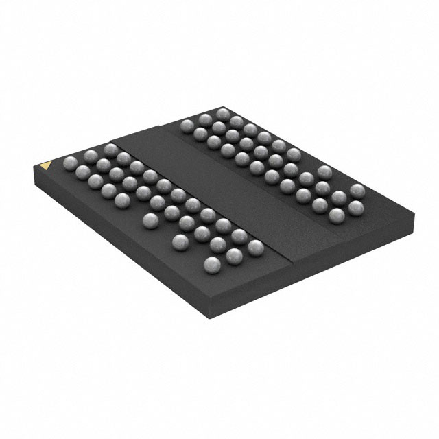
AS4C256M8D2-25BCN comes in a compact and standardized BGA (Ball Grid Array) package. This package provides reliable electrical connections and efficient heat dissipation.
Essence
The essence of AS4C256M8D2-25BCN lies in its ability to store and retrieve large amounts of data quickly and reliably, enhancing the overall performance of electronic devices.
Packaging/Quantity
AS4C256M8D2-25BCN is typically packaged in reels or trays, containing a specific quantity of chips per package. The exact packaging and quantity may vary depending on the manufacturer's specifications.
Specifications
- Memory Type: Synchronous DRAM (SDRAM)
- Capacity: 256 Megabits
- Speed: 25 Nanoseconds
- Organization: 256M x 8 bits
- Voltage Supply: 3.3 Volts
- Operating Temperature Range: -40°C to +85°C
- Package Type: BGA
Detailed Pin Configuration
AS4C256M8D2-25BCN has a total of 66 pins arranged in a specific configuration. The pin configuration is as follows:
- VDD
- DQ0
- DQ1
- DQ2
- DQ3
- DQ4
- DQ5
- DQ6
- DQ7
- VSS
- /RAS
- /CAS
- /WE
- /CS
- BA0
- BA1
- A0
- A1
- A2
- A3
- A4
- A5
- A6
- A7
- A8
- A9
- A10
- A11
- A12
- A13
- A14
- A15
- A16
- A17
- A18
- A19
- A20
- A21
- A22
- A23
- A24
- A25
- A26
- A27
- A28
- A29
- A30
- A31
- VDD
- VSS
- CLK
- CKE
- /CS2
- /CS3
- /CS4
- /CS5
- /CS6
- /CS7
- /CS8
- /CS9
- /CS10
- /CS11
- /CS12
- /CS13
- /CS14
- /CS15
Functional Features
- AS4C256M8D2-25BCN supports burst mode operations, allowing for efficient consecutive data transfers.
- It incorporates a self-refresh mode, enabling power-saving capabilities when the memory is not actively accessed.
- The chip features a programmable burst length, providing flexibility in data transfer operations.
- AS4C256M8D2-25BCN supports multiple banks, allowing simultaneous access to different sections of memory.
Advantages and Disadvantages
Advantages
- High-density storage capacity
- Fast data access speed
- Efficient burst mode operations
- Power-saving self-refresh mode
- Support for multiple banks
Disadvantages
- Relatively higher power consumption compared to other memory technologies
- Limited compatibility with older systems that do not support SDRAM
Working Principles
AS4C256M8D2-25BCN operates based on the principles of synchronous dynamic random-access memory (SDRAM). It stores data in a matrix of capacitors, where each capacitor represents a single bit of information. To read or write data, the chip utilizes clock signals to synchronize the timing of data transfers.
During read operations, the requested data is accessed by activating the appropriate row and column addresses. The data is then transferred to
技術ソリューションにおける AS4C256M8D2-25BCN の適用に関連する 10 件の一般的な質問と回答をリストします。
Question: What is the capacity of the AS4C256M8D2-25BCN memory module?
Answer: The AS4C256M8D2-25BCN has a capacity of 256 megabits (32 megabytes).Question: What is the operating voltage range for the AS4C256M8D2-25BCN?
Answer: The AS4C256M8D2-25BCN operates at a voltage range of 2.3V to 3.6V.Question: What is the maximum clock frequency supported by the AS4C256M8D2-25BCN?
Answer: The AS4C256M8D2-25BCN supports a maximum clock frequency of 250 MHz.Question: Is the AS4C256M8D2-25BCN compatible with DDR2 memory interfaces?
Answer: Yes, the AS4C256M8D2-25BCN is designed to be compatible with DDR2 memory interfaces.Question: Does the AS4C256M8D2-25BCN support burst mode operation?
Answer: Yes, the AS4C256M8D2-25BCN supports burst mode operation for efficient data transfer.Question: What is the access time of the AS4C256M8D2-25BCN?
Answer: The AS4C256M8D2-25BCN has an access time of 25 ns.Question: Can the AS4C256M8D2-25BCN be used in automotive applications?
Answer: Yes, the AS4C256M8D2-25BCN is suitable for automotive applications as it meets the required standards.Question: Does the AS4C256M8D2-25BCN have built-in error correction capabilities?
Answer: No, the AS4C256M8D2-25BCN does not have built-in error correction capabilities.Question: What is the package type of the AS4C256M8D2-25BCN?
Answer: The AS4C256M8D2-25BCN comes in a 60-ball FBGA (Fine-Pitch Ball Grid Array) package.Question: Is the AS4C256M8D2-25BCN RoHS compliant?
Answer: Yes, the AS4C256M8D2-25BCN is RoHS (Restriction of Hazardous Substances) compliant, ensuring environmental safety.