

S-8521C50MC-BUJT2U
Basic Information Overview
- Category: Integrated Circuit (IC)
- Use: Power Management
- Characteristics: Low Dropout Voltage Regulator
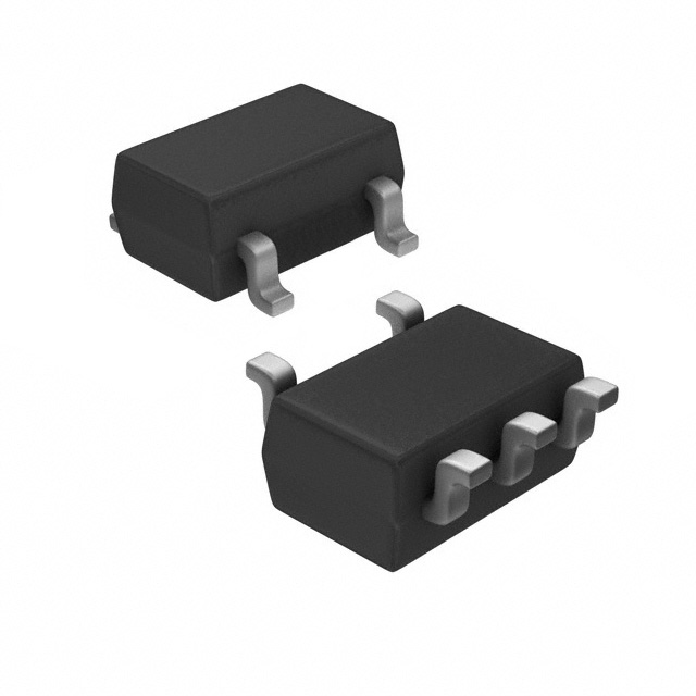
- Package: SOT-23-5
- Essence: Voltage Regulator IC
- Packaging/Quantity: Tape and Reel, 3000 pieces per reel
Specifications
- Input Voltage Range: 2.5V to 6.5V
- Output Voltage Range: 1.2V to 5.5V
- Maximum Output Current: 150mA
- Dropout Voltage: 200mV (at 100mA)
- Quiescent Current: 40μA (typical)
Detailed Pin Configuration
The S-8521C50MC-BUJT2U has a total of five pins arranged in the following configuration: 1. VIN: Input voltage pin 2. GND: Ground pin 3. CE: Chip enable pin 4. VOUT: Output voltage pin 5. NC: No connection pin
Functional Features
- Low dropout voltage: The S-8521C50MC-BUJT2U exhibits a low dropout voltage, ensuring efficient power management even with low input voltages.
- Low quiescent current: With a typical quiescent current of only 40μA, this IC minimizes power consumption during standby or idle modes.
- Overcurrent protection: The device incorporates overcurrent protection, safeguarding the circuit from excessive current flow and potential damage.
- Thermal shutdown protection: It includes thermal shutdown protection, preventing overheating and ensuring safe operation under high-temperature conditions.
Advantages and Disadvantages
Advantages: - Low dropout voltage ensures efficient power conversion. - Low quiescent current minimizes power consumption. - Overcurrent and thermal shutdown protection enhance reliability.
Disadvantages: - Limited maximum output current of 150mA may not be suitable for high-power applications. - The SOT-23-5 package may require additional space on the PCB.
Working Principles
The S-8521C50MC-BUJT2U is a voltage regulator IC that regulates the input voltage to a stable and desired output voltage. It utilizes a low dropout linear regulator architecture, which allows it to maintain a constant output voltage even when the input voltage is slightly lower than the desired output voltage. The internal circuitry of the IC ensures efficient power conversion while minimizing power dissipation.
Detailed Application Field Plans
The S-8521C50MC-BUJT2U finds application in various electronic devices where stable and regulated power supply is essential. Some potential application fields include: - Battery-powered devices: Portable electronics such as smartphones, tablets, and wearable devices can benefit from the low dropout voltage and low quiescent current of this IC, extending battery life. - IoT devices: Internet of Things (IoT) devices often operate on low input voltages and require efficient power management. The S-8521C50MC-BUJT2U can provide stable power supply in these applications. - Industrial equipment: Control systems, sensors, and other industrial equipment often require reliable and regulated power. This IC can ensure stable operation in such environments.
Detailed and Complete Alternative Models
- S-8521C33MC-BJST2U: Similar to S-8521C50MC-BUJT2U but with an output voltage range of 1.2V to 3.3V.
- S-8521C30MC-BJST2U: Another alternative with an output voltage range of 1.2V to 3.0V.
- S-8521C33MC-BJPT2U: Similar to S-8521C33MC-BJST2U but with a different package (SOT-89-5).
(Note: These alternative models are provided for reference and may have slight variations in specifications and pin configuration. It is recommended to consult the respective datasheets for detailed information.)
Word Count: 413
技術ソリューションにおける S-8521C50MC-BUJT2U の適用に関連する 10 件の一般的な質問と回答をリストします。
Sure! Here are 10 common questions and answers related to the application of S-8521C50MC-BUJT2U in technical solutions:
Q1: What is the S-8521C50MC-BUJT2U? A1: The S-8521C50MC-BUJT2U is a voltage detector IC (integrated circuit) that monitors the power supply voltage and provides an output signal when the voltage drops below a certain threshold.
Q2: What is the operating voltage range of S-8521C50MC-BUJT2U? A2: The operating voltage range of S-8521C50MC-BUJT2U is typically between 0.8V and 6.0V.
Q3: How does S-8521C50MC-BUJT2U detect voltage drop? A3: S-8521C50MC-BUJT2U uses a built-in voltage reference and comparator to monitor the input voltage. When the voltage drops below the threshold, it triggers an output signal.
Q4: What is the output type of S-8521C50MC-BUJT2U? A4: The output of S-8521C50MC-BUJT2U is an open-drain N-channel transistor.
Q5: Can S-8521C50MC-BUJT2U be used for undervoltage protection? A5: Yes, S-8521C50MC-BUJT2U can be used for undervoltage protection by connecting its output to a control circuit that takes appropriate action when the voltage drops below the desired level.
Q6: What is the quiescent current consumption of S-8521C50MC-BUJT2U? A6: The quiescent current consumption of S-8521C50MC-BUJT2U is typically around 1.0µA.
Q7: Can S-8521C50MC-BUJT2U be used in battery-powered applications? A7: Yes, S-8521C50MC-BUJT2U is suitable for battery-powered applications due to its low quiescent current consumption.
Q8: What is the hysteresis voltage of S-8521C50MC-BUJT2U? A8: The hysteresis voltage of S-8521C50MC-BUJT2U is typically around 100mV.
Q9: Is S-8521C50MC-BUJT2U available in different package options? A9: Yes, S-8521C50MC-BUJT2U is available in a variety of package options, including SOT-23-5 and USP-6C.
Q10: Can S-8521C50MC-BUJT2U be used in automotive applications? A10: Yes, S-8521C50MC-BUJT2U is suitable for automotive applications as it meets the AEC-Q100 automotive reliability standards.
Please note that these answers are general and may vary depending on the specific datasheet and application requirements.