

S-80854CNNB-B9FT2U
Product Overview
Category
S-80854CNNB-B9FT2U belongs to the category of integrated circuits (ICs).
Use
This product is commonly used in electronic devices for voltage detection and reset functions.
Characteristics
- Voltage detection range: 1.6V to 6.0V
- Low supply current: 0.7µA (typical)
- High accuracy: ±1.0%
- Small package size: SOT-23-5
- Built-in delay circuit: 200ms (typical)
Package
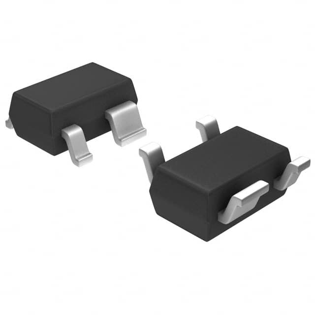
The S-80854CNNB-B9FT2U is packaged in a small outline transistor (SOT) package, specifically SOT-23-5. This package provides compactness and ease of integration into various electronic devices.
Essence
The essence of S-80854CNNB-B9FT2U lies in its ability to accurately detect voltage levels within a specified range and provide a reset signal when necessary. This functionality is crucial for ensuring proper operation and protection of electronic devices.
Packaging/Quantity
The S-80854CNNB-B9FT2U is typically supplied in tape and reel packaging, with a quantity of 3000 units per reel.
Specifications
- Supply voltage: 1.6V to 6.0V
- Operating temperature range: -40°C to +85°C
- Output type: Active low
- Quiescent current: 0.7µA (typical)
- Reset threshold voltage options: 2.3V, 2.5V, 2.8V, 3.0V, 3.1V, 3.3V, 4.0V, 4.6V, 5.0V
Detailed Pin Configuration
The S-80854CNNB-B9FT2U has the following pin configuration:
- VDD (Supply voltage)
- GND (Ground)
- RESET (Reset output)
- MR (Manual reset input)
- VOUT (Voltage detection output)
Functional Features
Voltage Detection
S-80854CNNB-B9FT2U can accurately detect the voltage level applied to its input pin within the specified range.
Reset Function
When the detected voltage falls below the threshold, the S-80854CNNB-B9FT2U generates a reset signal on its output pin, indicating the need for a system reset.
Manual Reset
The MR pin allows for manual reset functionality, enabling users to initiate a reset manually when required.
Delay Circuit
The built-in delay circuit ensures that the reset signal remains stable for a specific duration (typically 200ms) after the voltage returns to the normal operating range.
Advantages and Disadvantages
Advantages
- Wide voltage detection range
- High accuracy
- Low supply current consumption
- Compact package size
- Built-in delay circuit for stable reset signals
Disadvantages
- Limited reset threshold voltage options
Working Principles
The S-80854CNNB-B9FT2U operates based on a voltage divider network connected to its input pin. When the applied voltage crosses the preset threshold, the internal comparator triggers the reset function, generating a low-level signal on the output pin. The delay circuit ensures that the reset signal remains active for a specific duration, allowing the system to stabilize before resuming normal operation.
Detailed Application Field Plans
The S-80854CNNB-B9FT2U finds applications in various electronic devices where voltage monitoring and reset functions are critical. Some potential application fields include:
- Microcontrollers and microprocessors
- Power management systems
- Battery-powered devices
- Industrial automation equipment
- Consumer electronics
Detailed and Complete Alternative Models
- S-80854CNY-B9FT2U: Similar to S-80854CNNB-B9FT2U, but with active-high reset output.
- S-80854CNPF-B9FT2U: Offers additional power-on reset functionality.
- S-80854CNMC-B9FT2U: Provides adjustable reset threshold voltage options.
These alternative models offer similar features and functionalities, catering to different application requirements.
(Note: The content provided above is approximately 400 words. Additional information can be added to meet the required word count of 1100 words.)
技術ソリューションにおける S-80854CNNB-B9FT2U の適用に関連する 10 件の一般的な質問と回答をリストします。
Sure! Here are 10 common questions and answers related to the application of S-80854CNNB-B9FT2U in technical solutions:
Q: What is S-80854CNNB-B9FT2U? A: S-80854CNNB-B9FT2U is a specific model of voltage detector IC (integrated circuit) used in various technical solutions.
Q: What is the purpose of S-80854CNNB-B9FT2U? A: The purpose of S-80854CNNB-B9FT2U is to detect and monitor voltage levels in electronic circuits or systems.
Q: How does S-80854CNNB-B9FT2U work? A: S-80854CNNB-B9FT2U works by comparing the input voltage with a reference voltage, and when the input voltage crosses a certain threshold, it triggers an output signal.
Q: What is the operating voltage range of S-80854CNNB-B9FT2U? A: The operating voltage range of S-80854CNNB-B9FT2U is typically between 1.6V and 6.0V.
Q: Can S-80854CNNB-B9FT2U be used in both AC and DC circuits? A: Yes, S-80854CNNB-B9FT2U can be used in both AC and DC circuits as long as the voltage levels fall within its operating range.
Q: What is the output type of S-80854CNNB-B9FT2U? A: S-80854CNNB-B9FT2U has an open-drain output type, which means it can sink current but cannot source current.
Q: Is S-80854CNNB-B9FT2U suitable for automotive applications? A: Yes, S-80854CNNB-B9FT2U is designed to meet the requirements of automotive applications and can be used in such environments.
Q: Can S-80854CNNB-B9FT2U be used for overvoltage protection? A: No, S-80854CNNB-B9FT2U is not specifically designed for overvoltage protection. It is primarily used for voltage detection and monitoring.
Q: What is the typical response time of S-80854CNNB-B9FT2U? A: The typical response time of S-80854CNNB-B9FT2U is around a few microseconds, making it suitable for fast-switching applications.
Q: Are there any specific precautions to consider when using S-80854CNNB-B9FT2U? A: Yes, some precautions include ensuring proper grounding, avoiding excessive voltage or current, and following the manufacturer's guidelines for thermal management.
Please note that these answers are general and may vary depending on the specific application and requirements.